CPU_PROC_CMDDEC_34
Source: Verilog/CPU-BOARD-3202/circuit/CPU_PROC_CMDDEC_34.v
Where it sits (Simulation): ND120_TOP > ND120_CORE > ND3202D > CPU_15 > CPU_PROC_32 > CPU_PROC_CMDDEC_34
- instance path: CORE.CPU_BOARD.CPU.PROC.CMDDEC
Used in: CPU_PROC_32 (all tops)
Contains: PAL_44407A_EN, PAL_44408B_EN, PAL_44511A_EN
Module hierarchy - All modules
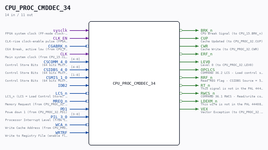
Schematic
Drawn from the Verilog: the yosys netlist of the Simulation (Verilator) build, instance CORE.CPU_BOARD.CPU.PROC.CMDDEC. Sub-modules are boxes (click the picture to open it full size; there every sub-module box links to its page, and every wire shows its Verilog name).
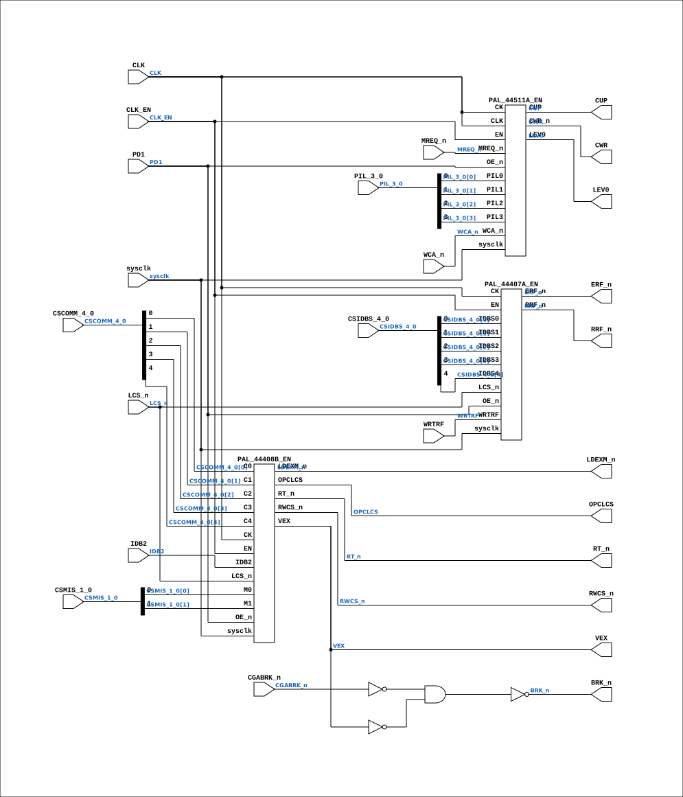
Description
ND120 CPU, MM&M CPU/PROC/CMDDEC COMMAND & IDB DECODE SHEET 34 of 50 Last reviewed: 1-DEC-2024 Ronny Hansen
Ports
| Direction | Width | Name | Description |
|---|---|---|---|
| input | 1 |
sysclk |
FPGA system clock (FF-mode clock-enable capture) |
| input | 1 |
CLK_EN |
CLK-rise clock-enable pulse (FPGA_FF_MODE, else 0) |
| input | 1 |
CGABRK_n (active low) |
CGA Break, active low (from CPU_PROC_CGA_33.CGABRK_n) |
| input | 1 |
CLK |
Main system clock (from CPU_15.CLK) |
| input | [4:0] |
CSCOMM_4_0 |
Control Store Bits (64 bits Microcode) (from CPU_PROC_32.CSBITS[36:32]) |
| input | [4:0] |
CSIDBS_4_0 |
Control Store Bits (64 bits Microcode) (from CPU_PROC_32.CSBITS[41:37]) |
| input | [1:0] |
CSMIS_1_0 |
Control Store Bits (64 bits Microcode) (from CPU_PROC_32.CSBITS[43:42]) |
| input | 1 |
IDB2 |
|
| input | 1 |
LCS_n (active low) |
LCS_n (LCS = Load Control Store) (from CPU_PROC_32.LCS_n) |
| input | 1 |
MREQ_n (active low) |
Memory Request (from CPU_PROC_32.MREQ_n) |
| input | 1 |
PD1 |
Powe down 1 (from CPU_PROC_32.PD1) |
| input | [3:0] |
PIL_3_0 |
Processor Interrupt Level (from CPU_PROC_CGA_33.PIL_3_0) |
| input | 1 |
WCA_n (active low) |
Write Cache Address (from CPU_PROC_32.WCA_n) |
| input | 1 |
WRTRF |
Write to Registry File (enable flag) |
| output | 1 |
BRK_n (active low) |
CPU Break Signal (to CPU_15.BRK_n) |
| output | 1 |
CUP |
Cache Updated (to CPU_PROC_32.CUP) |
| output | 1 |
CWR |
Cache Write (to CPU_PROC_32.CWR) |
| output | 1 |
ERF_n (active low) |
|
| output | 1 |
LEV0 |
Level 0 (to CPU_PROC_32.LEV0) |
| output | 1 |
OPCLCS |
COMMAND 36.2 LCS - Load control store from PROM and perform a Master Clear (to CPU_PROC_32.OPCLCS) |
| output | 1 |
RRF_n (active low) |
Read REG Flag - CSIDBS Source = 5 (REG) (to CPU_PROC_32.RRF_n) |
| output | 1 |
RT_n (active low) |
This signal is not in the PAL 44408B, but in the PAL 444608 (VXFIX). Use RT_n signal from DGA until we find out what the 44608A does with this signal. |
| output | 1 |
RWCS_n (active low) |
COMMAND 36.1 RWCS - Read/write control store as addressed by ADCS command (to CPU_PROC_32.RWCS_n) |
| output | 1 |
LDEXM_n (active low) |
This wire is not in the PAL 44408B, but in the PAL 444608 (VXFIX). Not sure what to do with this signal at the moment.. but brings it out here just in case.. |
| output | 1 |
VEX |
Vector Exception (to CPU_PROC_32.VEX) |
Verilog source
Verilog/CPU-BOARD-3202/circuit/CPU_PROC_CMDDEC_34.v on GitHub.
Show the Verilog of CPU_PROC_CMDDEC_34 (159 lines)
/**************************************************************************
** ND120 CPU, MM&M                                                       **
** CPU/PROC/CMDDEC                                                       **
** COMMAND & IDB DECODE                                                  **
** SHEET 34 of 50                                                        **
**                                                                       **
** Last reviewed: 1-DEC-2024                                             **
** Ronny Hansen                                                          **
***************************************************************************/
module CPU_PROC_CMDDEC_34 (
    input wire       sysclk,  //! FPGA system clock (FF-mode clock-enable capture)
    input wire       CLK_EN,  //! CLK-rise clock-enable pulse (FPGA_FF_MODE, else 0)

    input wire       CGABRK_n,  //! CGA Break, active low (from CPU_PROC_CGA_33.CGABRK_n)
    input wire       CLK,     //! Main system clock (from CPU_15.CLK)
    input wire [4:0] CSCOMM_4_0,  //! Control Store Bits  (64 bits Microcode) (from CPU_PROC_32.CSBITS[36:32])
    input wire [4:0] CSIDBS_4_0,  //! Control Store Bits  (64 bits Microcode) (from CPU_PROC_32.CSBITS[41:37])
    input wire [1:0] CSMIS_1_0,  //! Control Store Bits  (64 bits Microcode) (from CPU_PROC_32.CSBITS[43:42])
    input wire       IDB2,
    input wire       LCS_n,   //! LCS_n (LCS = Load Control Store) (from CPU_PROC_32.LCS_n)
    input wire       MREQ_n,  //! Memory Request (from CPU_PROC_32.MREQ_n)
    input wire       PD1,     //! Powe down 1 (from CPU_PROC_32.PD1)
    input wire [3:0] PIL_3_0,  //! Processor Interrupt Level (from CPU_PROC_CGA_33.PIL_3_0)
    input wire       WCA_n,   //! Write Cache Address (from CPU_PROC_32.WCA_n)
    input wire       WRTRF,  //! Write to Registry File (enable flag)

    output wire BRK_n,        //! CPU Break Signal (to CPU_15.BRK_n)
    output wire CUP,          //! Cache Updated (to CPU_PROC_32.CUP)
    output wire CWR,          //! Cache Write (to CPU_PROC_32.CWR)
    output wire ERF_n,
    output wire LEV0,         //! Level 0 (to CPU_PROC_32.LEV0)
    output wire OPCLCS,       //! COMMAND 36.2 LCS - Load control store from PROM and perform a Master Clear (to CPU_PROC_32.OPCLCS)
    output wire RRF_n,        //! Read REG Flag - CSIDBS Source = 5 (REG) (to CPU_PROC_32.RRF_n)
    output wire RT_n, // This signal is not in the PAL 44408B, but in the PAL 444608 (VXFIX). Use  RT_n signal from DGA until we find out what the 44608A does with this signal.
    output wire RWCS_n,       //! COMMAND 36.1 RWCS - Read/write control store as addressed by ADCS command (to CPU_PROC_32.RWCS_n)
    output wire LDEXM_n, // This wire is not in the PAL 44408B, but in the PAL 444608 (VXFIX). Not sure what to do with this signal at the moment.. but brings it out here just in case..
    output wire VEX           //! Vector Exception (to CPU_PROC_32.VEX)
);


  // P2 clock-domain conversion (docs/plan-fix-unconstrained-clocks.md): these
  // PALs register on CLK and sample the converted-domain microword
  // CSCOMM/CSMIS and IDB - part of the coupled clock group.
`ifdef FPGA_FF_MODE
  localparam CLK_CE = 1;
`else
  localparam CLK_CE = 0;
`endif

  /*******************************************************************************
   ** Here all normal components are defined                                     **
   *******************************************************************************/
  //NAND_GATE #(.BubblesMask(2'b11))
  //   GATES_1 (.input1(CGABRK_n),
  //            .input2(VEX),
  //            .result(BRK_n));

  assign BRK_n = ~(~CGABRK_n & ~VEX);


  /*******************************************************************************
   ** Here all sub-circuits are defined                                          **
   *******************************************************************************/

  //
  PAL_44407A_EN #(
      .USE_ENABLE(CLK_CE)
  ) PAL_44407_UERFIX (
      .sysclk(sysclk),  // FPGA system clock (USE_ENABLE=1)
      .EN(CLK_EN),      // CLK-rise clock-enable pulse (USE_ENABLE=1)

      .CK  (CLK),  // Clock signal
      .OE_n(PD1),  // OUTPUT ENABLE (active-low) for Q0-Q3

      .ERF_n(ERF_n),  // B0_n - ERF_n
      // .B1_n(),             // B1_n - (not connected)
      // .B2_n(),             // B2_n - (not connected)
      // .B3_n(),             // B3_n - (not connected)

      .IDBS0(CSIDBS_4_0[0]),  // I0 - CSIDBS0
      .IDBS1(CSIDBS_4_0[1]),  // I1 - CSIDBS1
      .IDBS2(CSIDBS_4_0[2]),  // I2 - CSIDBS2
      .IDBS3(CSIDBS_4_0[3]),  // I3 - CSIDBS3
      .IDBS4(CSIDBS_4_0[4]),  // I4 - CSIDBS4
      .WRTRF(WRTRF),          // I5 - WRTRF
      .LCS_n(LCS_n),          // I6 - LCS_n
      // .I7(1'b0),           // I7 is not connected

      .RRF_n(RRF_n)  // Q0_n - RRF_n
      // .Q1_n(),             // Q1_n - (not connected)
      // .Q2_n(),             // Q2_n - (not connected)
      // .Q3_n()              // Q3_n - (not connected)
  );

  // PAL_44608_UVXFIX should replace 44408B, but we have no PALASM source for it
  // Using the previois PAL_44408B instead

  // PAL_44408B VEXFIX
  PAL_44408B_EN #(
      .USE_ENABLE(CLK_CE)
  ) PAL_44408B_VEXFIX (
      .sysclk(sysclk),  // FPGA system clock (USE_ENABLE=1)
      .EN(CLK_EN),      // CLK-rise clock-enable pulse (USE_ENABLE=1)

      .CK  (CLK),  // Clock signal
      .OE_n(PD1),  // OUTPUT ENABLE (active-low) for Q0-Q5

      .C4(CSCOMM_4_0[4]),  // I0 - CSCOMM4
      .C3(CSCOMM_4_0[3]),  // I1 - CSCOMM3
      .C2(CSCOMM_4_0[2]),  // I2 - CSCOMM2
      .C1(CSCOMM_4_0[1]),  // I3 - CSCOMM1
      .C0(CSCOMM_4_0[0]),  // I4 - CSCOMM0
      .M1(CSMIS_1_0[1]),   // I5 - CSMIS1
      .M0(CSMIS_1_0[0]),   // I6 - CSMIS0
      // .I7(1'b0),        // I7 is not connected

      .LCS_n(LCS_n),  // B0_n - LCS_n
      .IDB2 (IDB2),   // B1_n - IDB2

      // .Q0_n(),         // Q0_n - (not connected)
      .LDEXM_n(LDEXM_n),  // Q1_n - LDEXM_n (not connected in n44608)
      .VEX    (VEX),      // Q2_n - VEX//
      .OPCLCS (OPCLCS),   // Q3_n - OPCLCS
      .RWCS_n (RWCS_n),   // Q4_n - RWCS_n
      .RT_n   (RT_n)      // Q5_n - RT_n (But only in 444608 VXFIX. Not in 44408B)// DONT USE SIGNAG FROM 44408 as its fixed high!
  );

  // PAL_44511_ULEV0
  PAL_44511A_EN #(
      .USE_ENABLE(CLK_CE)
  ) PAL_44511_ULEV0 (
      .sysclk(sysclk),  // FPGA system clock (USE_ENABLE=1)
      .EN(CLK_EN),      // CLK-rise clock-enable pulse (USE_ENABLE=1)

      .CK  (CLK),  // Clock signal
      .OE_n(PD1),  // OUTPUT ENABLE (active-low) for Q0-Q3

      .PIL0  (PIL_3_0[0]),  // I0 - PIL0
      .PIL1  (PIL_3_0[1]),  // I1 - PIL1
      .PIL2  (PIL_3_0[2]),  // I2 - PIL2
      .PIL3  (PIL_3_0[3]),  // I3 - PIL3
      .CLK   (CLK),         // I4 - CLK (same signal as CK)
      .MREQ_n(MREQ_n),      // I5 - MREQ_n
      .WCA_n (WCA_n),       // I6 - WCA_n
      // .I7(1'b0),         // I7 is not connected

      .CUP(CUP),  // Q0_n - CUP
      // .Q1_n(),  // Q1_n - (not connected)
      // .Q2_n(),  // Q2_n - (not connected)
      // .Q3_n(),  // Q3_n - (not connected)

      .CWR_n(CWR),  // B0_n - CWR_n   <== THIS LOOKS ODD, BUT IS CORRECT ACCORDING TO SCHEMATIC
      // .B1_n(),   // B1_n - (not connected)
      // .B2_n(),   // B2_n - (not connected)
      .LEV0 (LEV0)  // B3_n - LEV0
  );

endmodule