MEM_LBDIF_48
Source: Verilog/CPU-BOARD-3202/circuit/MEM_LBDIF_48.v
Where it sits (Simulation): ND120_TOP > ND120_CORE > ND3202D > MEM_43 > MEM_LBDIF_48
- instance path: CORE.CPU_BOARD.MEM.LBDIF
Used in: MEM_43 (all tops)
Contains: AM29C821 x2, PAL_44310D
Module hierarchy - All modules
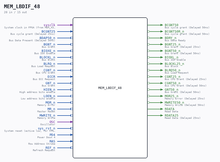
Schematic
Drawn from the Verilog: the yosys netlist of the Simulation (Verilator) build, instance CORE.CPU_BOARD.MEM.LBDIF. Sub-modules are boxes (click the picture to open it full size; there every sub-module box links to its page, and every wire shows its Verilog name).
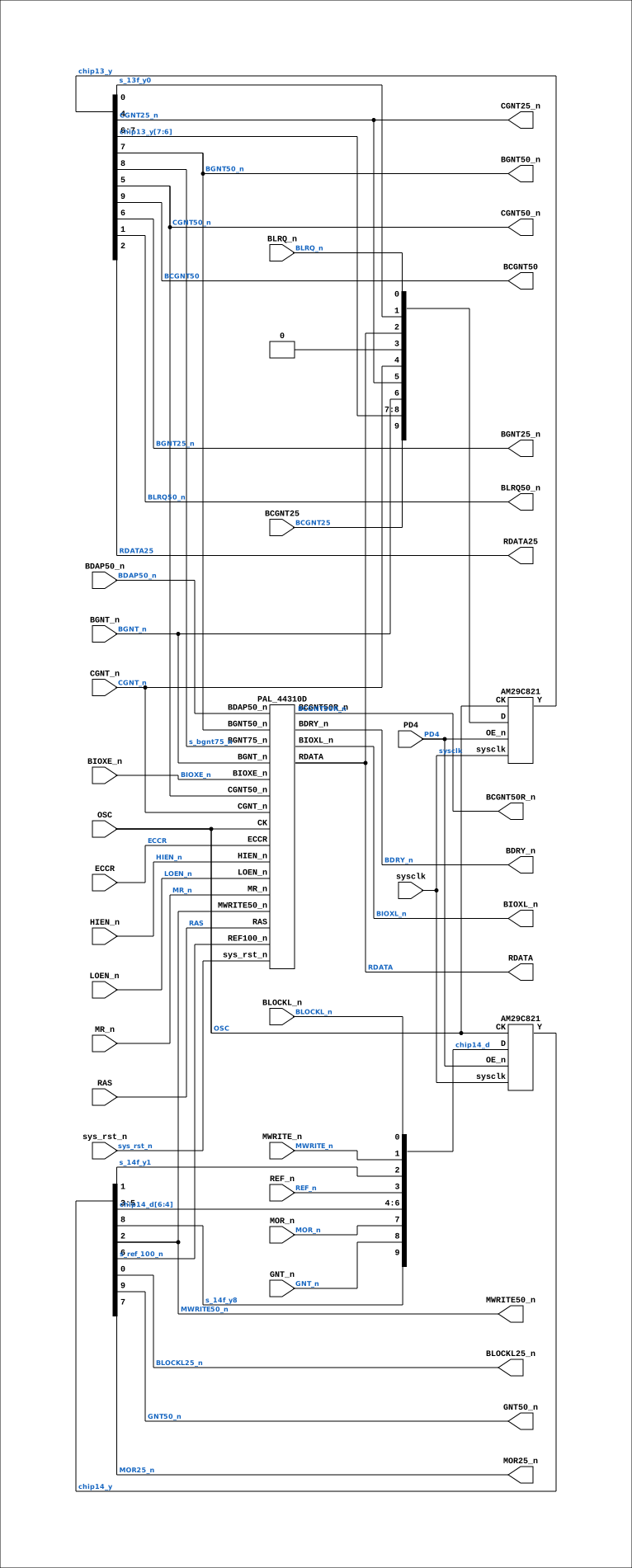
Description
ND120 CPU, MM&M MEM/LBDIF LOCAL BD CONTROL SHEET 48 of 50 Last reviewed: 2-FEB-2025 Ronny Hansen
Ports
| Direction | Width | Name | Description |
|---|---|---|---|
| input | 1 |
sysclk |
System clock in FPGA (from MEM_43.sysclk) |
| input | 1 |
BCGNT25 |
Bus cycle grant (Delayed 25ns) |
| input | 1 |
BDAP50_n (active low) |
Bus Data Present (Delayed 50ns) |
| input | 1 |
BGNT_n (active low) |
Bus Grant |
| input | 1 |
BIOXE_n (active low) |
Bus IOX Enable |
| input | 1 |
BLOCKL_n (active low) |
Bus Block |
| input | 1 |
BLRQ_n (active low) |
Bus Load Request |
| input | 1 |
CGNT_n (active low) |
Bus CPU Grant |
| input | 1 |
ECCR |
Bus ECC Request |
| input | 1 |
GNT_n (active low) |
Bus Grant |
| input | 1 |
HIEN_n (active low) |
High address bits enable |
| input | 1 |
LOEN_n (active low) |
Low address bits enable |
| input | 1 |
MOR_n (active low) |
Memory Error |
| input | 1 |
MR_n (active low) |
Master Reset |
| input | 1 |
MWRITE_n (active low) |
Memory Write |
| input | 1 |
OSC |
Oscillator |
| input | 1 |
sys_rst_n (active low) |
System reset (active low, for FPGA synthesis) |
| input | 1 |
PD4 |
Power Down 4 |
| input | 1 |
RAS |
Row Address Strobe |
| input | 1 |
REF_n (active low) |
Refresh Request |
| output | 1 |
BCGNT50 |
Bus cycle grant (Delayed 50ns) |
| output | 1 |
BCGNT50R_n (active low) |
Bus cycle grant (Delayed 50ns) |
| output | 1 |
BDRY_n (active low) |
Bus Data Ready |
| output | 1 |
BGNT25_n (active low) |
Bus Grant (Delayed 25ns) |
| output | 1 |
BGNT50_n (active low) |
Bus Grant (Delayed 50ns) |
| output | 1 |
BIOXL_n (active low) |
Bus IOX Enable |
| output | 1 |
BLOCKL25_n (active low) |
Bus Block |
| output | 1 |
BLRQ50_n (active low) |
Bus Load Request |
| output | 1 |
CGNT25_n (active low) |
Bus CPU Grant (Delayed 25ns) |
| output | 1 |
CGNT50_n (active low) |
Bus CPU Grant (Delayed 50ns) |
| output | 1 |
GNT50_n (active low) |
Bus Grant (Delayed 50ns) |
| output | 1 |
MOR25_n (active low) |
Memory Error (Delayed 25ns) |
| output | 1 |
MWRITE50_n (active low) |
Memory Write (Delayed 50ns) |
| output | 1 |
RDATA |
Read Data |
| output | 1 |
RDATA25 |
Read Data (Delayed 25ns) |
Verilog source
Verilog/CPU-BOARD-3202/circuit/MEM_LBDIF_48.v on GitHub.
Show the Verilog of MEM_LBDIF_48 (304 lines)
/**************************************************************************
** ND120 CPU, MM&M                                                       **
** MEM/LBDIF                                                             **
** LOCAL BD CONTROL                                                      **
** SHEET 48 of 50                                                        **
**                                                                       **
** Last reviewed: 2-FEB-2025                                             **
** Ronny Hansen                                                          **
***************************************************************************/

module MEM_LBDIF_48 (
    // Input signals
    input sysclk,    //! System clock in FPGA (from MEM_43.sysclk)
    input BCGNT25,   //! Bus cycle grant (Delayed 25ns)
    input BDAP50_n,  //! Bus Data Present (Delayed 50ns)
    input BGNT_n,    //! Bus Grant
    input BIOXE_n,   //! Bus IOX Enable
    input BLOCKL_n,  //! Bus Block
    input BLRQ_n,    //! Bus Load Request
    input CGNT_n,    //! Bus CPU Grant
    input ECCR,      //! Bus ECC Request
    input GNT_n,     //! Bus Grant
    input HIEN_n,    //! High address bits enable
    input LOEN_n,    //! Low address bits enable
    input MOR_n,     //! Memory Error
    input MR_n,      //! Master Reset
    input MWRITE_n,  //! Memory Write
    input OSC,       //! Oscillator
    input sys_rst_n, //! System reset (active low, for FPGA synthesis)
    input PD4,       //! Power Down 4
    input RAS,       //! Row Address Strobe
    input REF_n,     //! Refresh Request

    // Output signals
    output BCGNT50,     //! Bus cycle grant (Delayed 50ns)
    output BCGNT50R_n,  //! Bus cycle grant (Delayed 50ns)
    output BDRY_n,      //! Bus Data Ready
    output BGNT25_n,    //! Bus Grant (Delayed 25ns)
    output BGNT50_n,    //! Bus Grant (Delayed 50ns)
    output BIOXL_n,     //! Bus IOX Enable
    output BLOCKL25_n,  //! Bus Block
    output BLRQ50_n,    //! Bus Load Request
    output CGNT25_n,    //! Bus CPU Grant (Delayed 25ns)
    output CGNT50_n,    //! Bus CPU Grant (Delayed 50ns)
    output GNT50_n,     //! Bus Grant (Delayed 50ns)
    output MOR25_n,     //! Memory Error (Delayed 25ns)
    output MWRITE50_n,  //! Memory Write (Delayed 50ns)
    output RDATA,       //! Read Data
    output RDATA25      //! Read Data (Delayed 25ns)
);

  /*******************************************************************************
   ** The wires are defined here                                                 **
   *******************************************************************************/
  wire s_13f_y0;
  wire s_14f_y1;
  wire s_14f_y3;
  wire s_14f_y4;
  wire s_14f_y5;
  wire s_14f_y8;
  wire s_bcgnt25;
  wire s_bcgnt50_out;
  wire s_bcgnt50r_n_out;
  wire s_bdap50_n;
  wire s_bdry_n_out;
  wire s_bgnt_n;
  wire s_bgnt50_n_out;
  wire s_bgnt50_n;
  wire s_bgnt75_n;
  wire s_bioxe_n;
  wire s_bioxl_n_out;
  wire s_blockl_n;
  wire s_blockl25_n_out;
  wire s_blrq_n;
  wire s_blrq50_n_out;
  wire s_cgnt_n;
  wire s_cgnt25_n_out;
  wire s_cgnt50_n_out;
  wire s_eccr;
  wire s_gnt_n;
  wire s_gnt50_n_out;
  wire s_hien_n;
  wire s_loen_n;
  wire s_mor_n;
  wire s_mor25_n_out;
  wire s_mr_n;
  wire s_mwrite_n;
  wire s_mwrite50_n;
  wire s_osc;
  wire s_pd4;
  wire s_ras;
  wire s_rdata_out;
  wire s_rdata25_out;
  wire s_ref_100_n;
  wire s_ref_n;

  wire [9:0] chip13_d;
  wire [9:0] chip13_y;

  wire [9:0] chip14_d;
  wire [9:0] chip14_y;

  /*******************************************************************************
   ** Here all input connections are defined                                     **
   *******************************************************************************/
  assign s_hien_n       = HIEN_n;
  assign s_pd4          = PD4;
  assign s_eccr         = ECCR;
  assign s_loen_n       = LOEN_n;
  assign s_blrq_n       = BLRQ_n;
  assign s_mwrite_n     = MWRITE_n;
  assign s_ref_n        = REF_n;
  assign s_mor_n        = MOR_n;
  assign s_bgnt_n       = BGNT_n;
  assign s_mr_n         = MR_n;
  assign s_bioxe_n      = BIOXE_n;
  assign s_bdap50_n     = BDAP50_n;
  assign s_bcgnt25      = BCGNT25;
  assign s_ras          = RAS;
  assign s_blockl_n     = BLOCKL_n;
  assign s_gnt_n        = GNT_n;
  assign s_osc          = OSC;
  assign s_cgnt_n       = CGNT_n;

  /*******************************************************************************
   ** Here all output connections are defined                                    **
   *******************************************************************************/
  assign BCGNT50        = s_bcgnt50_out;
  assign BCGNT50R_n     = s_bcgnt50r_n_out;
  assign BDRY_n         = s_bdry_n_out;
  assign BGNT25_n       = s_bgnt50_n_out;
  assign BGNT50_n       = s_bgnt50_n;
  assign BIOXL_n        = s_bioxl_n_out;
  assign BLOCKL25_n     = s_blockl25_n_out;
  assign BLRQ50_n       = s_blrq50_n_out;
  assign CGNT25_n       = s_cgnt25_n_out;
  assign CGNT50_n       = s_cgnt50_n_out;
  assign GNT50_n        = s_gnt50_n_out;
  assign MOR25_n        = s_mor25_n_out;
  assign MWRITE50_n     = s_mwrite50_n;
  assign RDATA          = s_rdata_out;
  assign RDATA25        = s_rdata25_out;

  /*******************************************************************************
   ** Here all sub-circuits are defined                                          **
   *******************************************************************************/

  /************ CHIP 13F ************/

  /*

      // Input
      .D0(s_blrq_n),
      .D1(s_13f_y0),
      .D2(s_rdata_out),
      .D3(1'b0), // n.c.
      .D4(s_cgnt_n),
      .D5(s_cgnt25_n_out),
      .D6(s_bgnt_n),
      .D7(s_bgnt50_n_out),
      .D8(s_bgnt50_n),
      .D9(s_bcgnt25),

      // Output
      .Y0(s_13f_y0),
      .Y1(s_blrq50_n_out),
      .Y2(s_rdata25_out),
      .Y3(),
      .Y4(s_cgnt25_n_out),
      .Y5(s_cgnt50_n_out),
      .Y6(s_bgnt50_n_out),
      .Y7(s_bgnt50_n),
      .Y8(s_bgnt75_n),
      .Y9(s_bcgnt50_out)

  */

  // D - 10 Input signals
  assign chip13_d[0]    = s_blrq_n;
  assign chip13_d[1]    = s_13f_y0;
  assign chip13_d[2]    = s_rdata_out;
  assign chip13_d[3]    = 1'b0;
  assign chip13_d[4]    = s_cgnt_n;
  assign chip13_d[5]    = s_cgnt25_n_out;  // y4 looped back
  assign chip13_d[6]    = s_bgnt_n;
  assign chip13_d[7]    = s_bgnt50_n_out;  // y6 looped back
  assign chip13_d[8]    = s_bgnt50_n;  // y7 looped back
  assign chip13_d[9]    = s_bcgnt25;

  // Y - 10 Output signals
  assign s_13f_y0       = chip13_y[0];
  assign s_blrq50_n_out = chip13_y[1];
  assign s_rdata25_out  = chip13_y[2];

  // Unused wire, this to keep LINTER happy and not complaining about chip13_y[3] bit not read
  (* keep = "true", DONT_TOUCH = "true" *) wire notused_chip13y3 = chip13_y[3];

  assign s_cgnt25_n_out = chip13_y[4];
  assign s_cgnt50_n_out = chip13_y[5];
  assign s_bgnt50_n_out = chip13_y[6];
  assign s_bgnt50_n     = chip13_y[7];
  assign s_bgnt75_n     = chip13_y[8];
  assign s_bcgnt50_out  = chip13_y[9];


  AM29C821 CHIP_13F (
      .sysclk(sysclk),
      .CK(s_osc),
      .OE_n(s_pd4),
      .D(chip13_d),
      .Y(chip13_y)
  );


  /************ CHIP 14F ************/
  /*
      .D0  (s_blockl_n),
      .D1  (s_mwrite_n),
      .D2  (s_14f_y1),
      .D3  (s_ref_n),
      .D4  (s_14f_y3),
      .D5  (s_14f_y4),
      .D6  (s_14f_y5),
      .D7  (s_mor_n),
      .D8  (s_gnt_n),
      .D9  (s_14f_y8),

      .Y0  (s_blockl25_n_out),
      .Y1  (s_14f_y1),
      .Y2  (s_mwrite50_n),
      .Y3  (s_14f_y3),
      .Y4  (s_14f_y4),
      .Y5  (s_14f_y5),
      .Y6  (s_ref_100_n),
      .Y7  (s_mor25_n_out),
      .Y8  (s_14f_y8),
      .Y9  (s_gnt50_n_out)
    */
  assign chip14_d[0]      = s_blockl_n;
  assign chip14_d[1]      = s_mwrite_n;
  assign chip14_d[2]      = s_14f_y1;
  assign chip14_d[3]      = s_ref_n;
  assign chip14_d[4]      = s_14f_y3;  // y3
  assign chip14_d[5]      = s_14f_y4;  // y4
  assign chip14_d[6]      = s_14f_y5;  // y5
  assign chip14_d[7]      = s_mor_n;
  assign chip14_d[8]      = s_gnt_n;
  assign chip14_d[9]      = s_14f_y8;  // y8


  assign s_blockl25_n_out = chip14_y[0];
  assign s_14f_y1         = chip14_y[1];
  assign s_mwrite50_n     = chip14_y[2];
  assign s_14f_y3         = chip14_y[3];
  assign s_14f_y4         = chip14_y[4];
  assign s_14f_y5         = chip14_y[5];
  assign s_ref_100_n      = chip14_y[6];
  assign s_mor25_n_out    = chip14_y[7];
  assign s_14f_y8         = chip14_y[8];
  assign s_gnt50_n_out    = chip14_y[9];

  AM29C821 CHIP_14F (
      .sysclk(sysclk),
      .CK(s_osc),
      .OE_n(s_pd4),
      .D(chip14_d),
      .Y(chip14_y)
  );

  /************ PAL chip 3F ************/

  PAL_44310D PAL_44310_ULBDIF (
      // Clock and reset (added for FPGA synthesis)
      .CK      (s_osc),           // Clock
      .sys_rst_n(sys_rst_n),      // System reset

      // Inputs
      .HIEN_n  (s_hien_n),        // I0
      .BGNT_n  (s_bgnt_n),        // I1
      .CGNT_n  (s_cgnt_n),        // I2
      .LOEN_n  (s_loen_n),        // I3
      .CGNT50_n(s_cgnt50_n_out),  // I4
      .ECCR    (s_eccr),          // I5
      .BGNT50_n(s_bgnt50_n),      // I6
      .BGNT75_n(s_bgnt75_n),      // I7
      .BDAP50_n(s_bdap50_n),      // I8
      .MR_n    (s_mr_n),          // I9

      .BDRY_n    (s_bdry_n_out),   // B0 Output
      .BIOXL_n   (s_bioxl_n_out),  // B1 Output
      .RAS       (s_ras),          // B2
      .REF100_n  (s_ref_100_n),    // B3
      .BIOXE_n   (s_bioxe_n),      // B4
      .MWRITE50_n(s_mwrite50_n),   // B5


      .BCGNT50R_n(s_bcgnt50r_n_out),  // Y0 Output
      .RDATA     (s_rdata_out)        // Y1 Output
  );


endmodule