BIF_BCTL_BDRV_7
Source: Verilog/CPU-BOARD-3202/circuit/BIF_BCTL_BDRV_7.v
Where it sits (Simulation): ND120_TOP > ND120_CORE > ND3202D > BIF_5 > BIF_BCTL_6 > BIF_BCTL_BDRV_7
- instance path: CORE.CPU_BOARD.BIF.BCTL.BDRV
Used in: BIF_BCTL_6 (all tops)
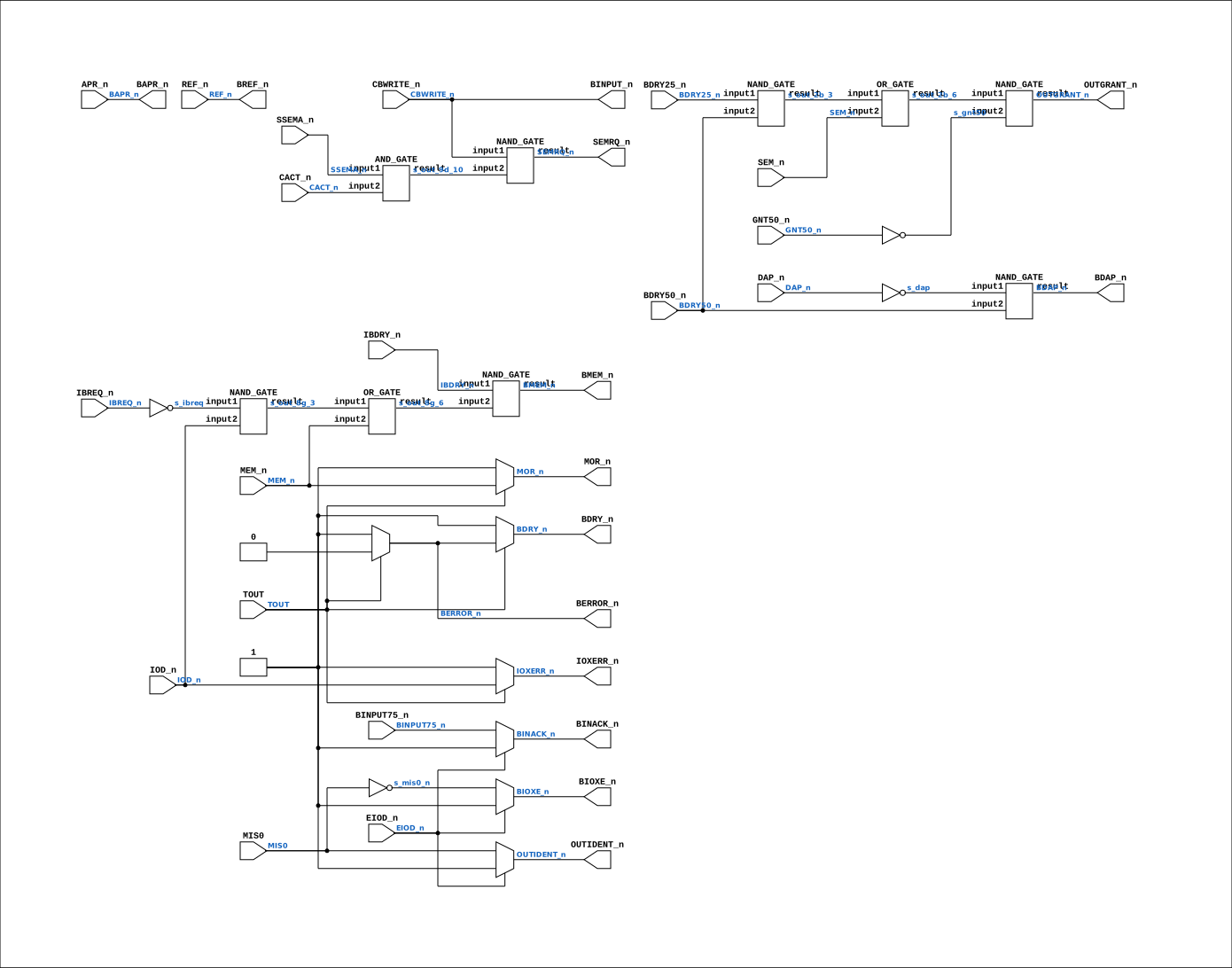
Contains: AND_GATE, NAND_GATE x6, OR_GATE x2
Module hierarchy - All modules
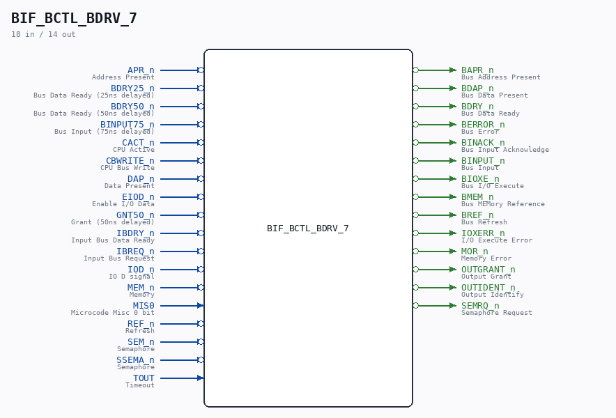
Schematic
Drawn from the Verilog: the yosys netlist of the Simulation (Verilator) build, instance CORE.CPU_BOARD.BIF.BCTL.BDRV. Sub-modules are boxes (click the picture to open it full size; there every sub-module box links to its page, and every wire shows its Verilog name).
Description
ND120 CPU, MM&M BIF/BCTL/BDRV BUS DRIVER SHEET 7 of 50 Last reviewed: 22-MAR-2024 Ronny Hansen
Ports
| Direction | Width | Name | Description |
|---|---|---|---|
| input | 1 |
APR_n (active low) |
Address Present |
| input | 1 |
BDRY25_n (active low) |
Bus Data Ready (25ns delayed) |
| input | 1 |
BDRY50_n (active low) |
Bus Data Ready (50ns delayed) |
| input | 1 |
BINPUT75_n (active low) |
Bus Input (75ns delayed) |
| input | 1 |
CACT_n (active low) |
CPU Active |
| input | 1 |
CBWRITE_n (active low) |
CPU Bus Write |
| input | 1 |
DAP_n (active low) |
Data Present |
| input | 1 |
EIOD_n (active low) |
Enable I/O Data |
| input | 1 |
GNT50_n (active low) |
Grant (50ns delayed) |
| input | 1 |
IBDRY_n (active low) |
Input Bus Data Ready |
| input | 1 |
IBREQ_n (active low) |
Input Bus Request |
| input | 1 |
IOD_n (active low) |
IO D signal |
| input | 1 |
MEM_n (active low) |
Memory |
| input | 1 |
MIS0 |
Microcode Misc 0 bit |
| input | 1 |
REF_n (active low) |
Refresh |
| input | 1 |
SEM_n (active low) |
Semaphore |
| input | 1 |
SSEMA_n (active low) |
Semaphore |
| input | 1 |
TOUT |
Timeout |
| output | 1 |
BAPR_n (active low) |
Bus Address Present |
| output | 1 |
BDAP_n (active low) |
Bus Data Present |
| output | 1 |
BDRY_n (active low) |
Bus Data Ready |
| output | 1 |
BERROR_n (active low) |
Bus Error |
| output | 1 |
BINACK_n (active low) |
Bus Input Acknowledge |
| output | 1 |
BINPUT_n (active low) |
Bus Input |
| output | 1 |
BIOXE_n (active low) |
Bus I/O Execute |
| output | 1 |
BMEM_n (active low) |
Bus MEMory Reference |
| output | 1 |
BREF_n (active low) |
Bus Refresh |
| output | 1 |
IOXERR_n (active low) |
I/O Execute Error |
| output | 1 |
MOR_n (active low) |
Memory Error |
| output | 1 |
OUTGRANT_n (active low) |
Output Grant |
| output | 1 |
OUTIDENT_n (active low) |
Output Identify |
| output | 1 |
SEMRQ_n (active low) |
Semaphore Request |
Verilog source
Verilog/CPU-BOARD-3202/circuit/BIF_BCTL_BDRV_7.v on GitHub.
Show the Verilog of BIF_BCTL_BDRV_7 (258 lines)
/**************************************************************************
** ND120 CPU, MM&M                                                       **
** BIF/BCTL/BDRV                                                         **
** BUS DRIVER                                                            **
** SHEET 7 of 50                                                         **
**                                                                       **
** Last reviewed: 22-MAR-2024                                            **
** Ronny Hansen                                                          **
***************************************************************************/

module BIF_BCTL_BDRV_7 (
    input APR_n,       //! Address Present
    input BDRY25_n,    //! Bus Data Ready (25ns delayed)
    input BDRY50_n,    //! Bus Data Ready (50ns delayed)
    input BINPUT75_n,  //! Bus Input (75ns delayed)
    input CACT_n,      //! CPU Active
    input CBWRITE_n,   //! CPU Bus Write
    input DAP_n,       //! Data Present
    input EIOD_n,      //! Enable I/O Data
    input GNT50_n,     //! Grant (50ns delayed)
    input IBDRY_n,     //! Input Bus Data Ready
    input IBREQ_n,     //! Input Bus Request
    input IOD_n,       //! IO D signal
    input MEM_n,       //! Memory
    input MIS0,        //! Microcode Misc 0 bit
    input REF_n,       //! Refresh
    input SEM_n,       //! Semaphore
    input SSEMA_n,     //! Semaphore
    input TOUT,        //! Timeout

    output BAPR_n,     //! Bus Address Present
    output BDAP_n,     //! Bus Data Present
    output BDRY_n,     //! Bus Data Ready
    output BERROR_n,   //! Bus Error
    output BINACK_n,   //! Bus Input Acknowledge
    output BINPUT_n,   //! Bus Input
    output BIOXE_n,    //! Bus I/O Execute
    output BMEM_n,     //! Bus MEMory Reference
    output BREF_n,     //! Bus Refresh
    output IOXERR_n,   //! I/O Execute Error
    output MOR_n,      //! Memory Error
    output OUTGRANT_n, //! Output Grant
    output OUTIDENT_n, //! Output Identify
    output SEMRQ_n     //! Semaphore Request
);


// ND-06.016.01.PDF page 140
//
// BMEM_N serves two important functions.
// It enables the memory system for further operations and ”freezes” the DMA request status on the DMA controllers
// (0=Read from MEM to BUS)
//
// The ”freezing” of the DMA request status is done to ensure a stabilized test condition for the INGRANT/OUTGRANT search chain.
// (It might happen that a DMA controller activates its request simultaneously with the reception of INGRANT.)
// That is, leading edge of BMEM_n is the last chance for a DMA request to be served by the current INGRANT/OUTGRANT search.


  /*******************************************************************************
   ** The wires are defined here                                                 **
   *******************************************************************************/
  wire s_iod_n;
  wire s_eiod_n;
  wire s_outident_n;
  wire s_bioxe_n;
  wire s_binack_n;
  wire s_ioxerr_n;
  wire s_mor_n;
  wire s_bdry_n;
  wire s_ibdry_n;
  wire s_sem_n;
  wire s_cbwrite_n;

  wire s_out_8g_6;
  wire s_gnt50;
  wire s_gnd;
  wire s_mis0_n;
  wire s_dap_n;
  wire s_ssema_n;
  wire s_cact_n;
  wire s_bmem_n;
  wire s_mem_n;
  wire s_out_2a_8;
  wire s_berror_n;
  wire s_gnt50_n;
  wire s_out_2b_8;
  wire s_ibreq;
  wire s_out_8g_3;
  wire s_ref_n;
  wire s_apr_n;
  wire s_ibreq_n;
  wire s_bdry25_n;
  wire s_bdry50_n;
  wire s_bdap_n;
  wire s_binput75_n;
  wire s_out_2b_3;
  wire s_tout;
  wire s_dap;
  wire s_out_9d_10;
  wire s_mis0;
  wire s_out_2b_6;

  /*******************************************************************************
   ** Here all input connections are defined                                     **
   *******************************************************************************/
  assign s_apr_n      = APR_n;
  assign s_bdry25_n   = BDRY25_n;
  assign s_bdry50_n   = BDRY50_n;
  assign s_binput75_n = BINPUT75_n;
  assign s_cact_n     = CACT_n;
  assign s_cbwrite_n  = CBWRITE_n;
  assign s_dap_n      = DAP_n;
  assign s_gnt50_n    = GNT50_n;
  assign s_ibdry_n    = IBDRY_n;
  assign s_ibreq_n    = IBREQ_n;
  assign s_iod_n      = IOD_n;
  assign s_eiod_n     = EIOD_n;
  assign s_mem_n      = MEM_n;
  assign s_mis0       = MIS0;
  assign s_ref_n      = REF_n;
  assign s_sem_n      = SEM_n;
  assign s_ssema_n    = SSEMA_n;
  assign s_tout       = TOUT;

  /*******************************************************************************
   ** Here all output connections are defined                                    **
   *******************************************************************************/
  assign BAPR_n       = s_apr_n;
  assign BDAP_n       = s_bdap_n;
  assign BDRY_n       = s_bdry_n;
  assign BERROR_n     = s_berror_n;
  assign BINACK_n     = s_binack_n;
  assign BINPUT_n     = s_cbwrite_n;
  assign BIOXE_n      = s_bioxe_n;
  assign BMEM_n       = s_bmem_n;
  assign BREF_n       = s_ref_n;
  assign IOXERR_n     = s_ioxerr_n;
  assign MOR_n        = s_mor_n;
  assign OUTGRANT_n   = s_out_2b_8;
  assign OUTIDENT_n   = s_outident_n;
  assign SEMRQ_n      = s_out_2a_8;

  /*******************************************************************************
   ** Here all in-lined components are defined                                   **
   *******************************************************************************/

  // Ground
  assign s_gnd        = 1'b0;

  // Signal inverters
  assign s_gnt50      = ~s_gnt50_n;
  assign s_mis0_n     = ~s_mis0;
  assign s_ibreq      = ~s_ibreq_n;
  assign s_dap        = ~s_dap_n;

  /*******************************************************************************
   ** Here all normal components are defined                                     **
   *******************************************************************************/
  OR_GATE #(
      .BubblesMask(2'b11)
  ) GATES_1 (
      .input1(s_out_2b_3),
      .input2(s_sem_n),
      .result(s_out_2b_6)
  );

  NAND_GATE #(
      .BubblesMask(2'b00)
  ) GATES_2 (
      .input1(s_cbwrite_n),
      .input2(s_out_9d_10),
      .result(s_out_2a_8)
  );

  NAND_GATE #(
      .BubblesMask(2'b00)
  ) GATES_3 (
      .input1(s_out_2b_6),
      .input2(s_gnt50),
      .result(s_out_2b_8)
  );

  NAND_GATE #(
      .BubblesMask(2'b00)
  ) GATES_4 (
      .input1(s_ibreq),
      .input2(s_iod_n),
      .result(s_out_8g_3)
  );

  OR_GATE #(
      .BubblesMask(2'b11)
  ) GATES_5 (
      .input1(s_out_8g_3),
      .input2(s_mem_n),
      .result(s_out_8g_6)
  );

  AND_GATE #(
      .BubblesMask(2'b11)
  ) GATES_6 (
      .input1(s_ssema_n),
      .input2(s_cact_n),
      .result(s_out_9d_10)
  );

  NAND_GATE #(
      .BubblesMask(2'b00)
  ) GATES_7 (
      .input1(s_dap),
      .input2(s_bdry50_n),
      .result(s_bdap_n)
  );

  NAND_GATE #(
      .BubblesMask(2'b00)
  ) GATES_8 (
      .input1(s_ibdry_n),
      .input2(s_out_8g_6),
      .result(s_bmem_n)
  );

  NAND_GATE #(
      .BubblesMask(2'b00)
  ) GATES_9 (
      .input1(s_bdry25_n),
      .input2(s_bdry50_n),
      .result(s_out_2b_3)
  );


  /*******************************************************************************
   ** Here all sub-circuits are defined                                          **
   *******************************************************************************/

   // Refactored away the 74F241 CHIP 3A into logic

  // pull OUTIDENT_n high if EIOD_n is high (giving 3 state output on 74241-Y1)
  assign s_outident_n = s_eiod_n ? 1'b1 : s_mis0; // PULL UP

  // Changed from the original schematic - Pull BIOXE and BINACK high instead of three-state. Maybe there are some pull-up resisters somewhere else?
  // pull BIOXE_n high if EOID_n is high (giving 3 state output on 74241-Y1)
  assign s_bioxe_n = s_eiod_n ? 1'b1 : s_mis0_n; // No pull up here.. somewhere else ??

  // pull BINACK_n high if EOID_n is high (giving 3 state output on 74241-Y1)
  assign s_binack_n =  s_eiod_n ? 1'b1 : s_binput75_n; // No pull up here.. somewhere else ??

  // 4th output of 74241-Y1 is not connected

  // pull IOXERR_n, MOR_n,BERROR_n and BDRY_n high if TOUT is low (giving 3 state output on 74241-Y2)
  assign s_ioxerr_n = s_tout ? s_iod_n : 1'b1;  // PULL UP
  assign s_mor_n    = s_tout ? s_mem_n : 1'b1;  // PULL UP
  assign s_berror_n = s_tout ? s_gnd : 1'b1;    // No pull up here.. somewhere else ??
  assign s_bdry_n   = s_tout ? s_berror_n: 1'b1;// No pull up here.. somewhere else ??


endmodule