PANCAL_68705_CLOCK
Source: Verilog/CPU-BOARD-3202/circuit/PANCAL_68705_CLOCK.v
Where it sits (Nexys): nd120_nexys4ddr_top > ND120_CORE > ND3202D > IO_37 > IO_PANCAL_40 > PANCAL_68705_CLOCK
- instance path: CORE.CPU_BOARD.IO.PANCAL.CHIP_35C
Used in: IO_PANCAL_40 (Nexys, MiSTer, MEGA65 R6, MEGA65 R3, QMTECH)
Contains: no other modules.
Module hierarchy - All modules
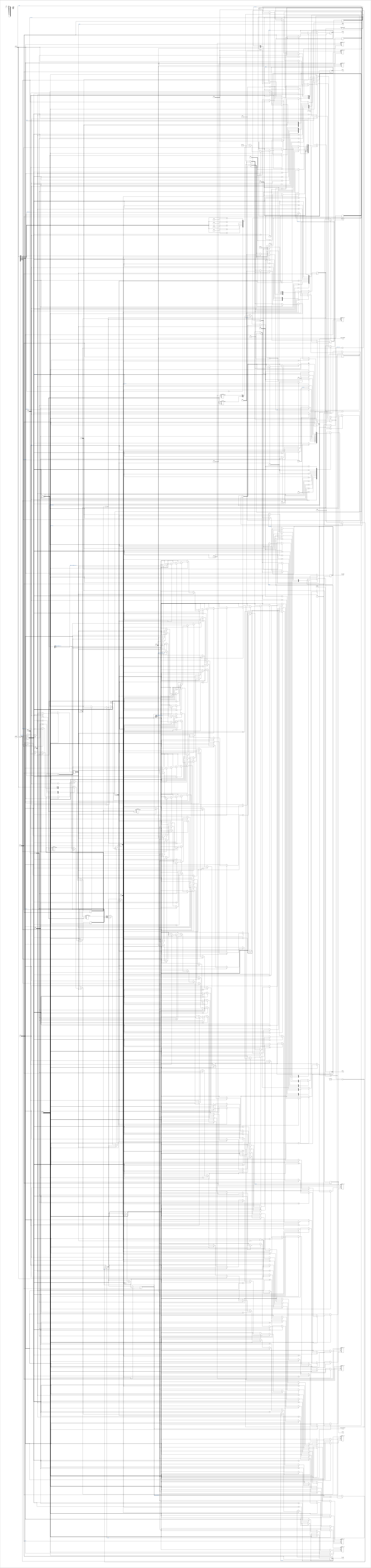
Schematic
Drawn from the Verilog: the yosys netlist of the Nexys 4 DDR build, instance CORE.CPU_BOARD.IO.PANCAL.CHIP_35C. Sub-modules are boxes (click the picture to open it full size; there every sub-module box links to its page, and every wire shows its Verilog name).
Description
ND120 CPU, MM&M PANCAL_68705_CLOCK Behavioural stand-in for the MC68705U3 panel processor (44A/35C) and the MM58274 calendar chip (34A) on sheet 40 - CLOCK PATH ONLY. Source of truth: the ROM dump Code/68705/MC68705U3_35C.BIN, disassembled by hand (28-AUG-2026). Addresses below are ROM addresses. Sheet 40 (Code/68705/3202D_PANCAL_SHEET40.png) gives the pin names. WHAT THE REAL CHIP DOES (clock part) Idle loop 0x014E: polls PD7 = EMP~ (DGA FIFO "not empty"). Read a FIFO byte 0x09BC: BCLR 3,PORTB (RMM~ low) ; LDA PORTA ; BSET 3,PORTB. The DGA pops one byte per XCLK while RMM~ is low. Command byte = high byte of the TRR PANC operand (microcode RPANC o1045 does IDBS,SWAP + LDPANC twice: A[15:8] first, then A[7:0]): bit 5 = PANC bit 13 "read request" bit 3 = PANC bit 11, always 0 for the clock bit 2:0 = PFUNC (PANC bits 10:8) Dispatch 0x04D8: bit3=1 -> display/text commands (RAM only, never answered). bit3=0 -> 0x06BE, the clock path: PORTC[2:0] = PFUNC (STAT2:0 -> PANS bits 10:8) if PFUNC bit2 == 0: RTS (PFUNC 0-3: no answer at all) BCLR 5,PORTB (STAT4 low = busy) idx = (PFUNC & 3) ^ 3 (RAM $47+idx) bit5=0 (CPU WRITES the clock): BCLR 6,PORTB (READ=0); byte = next FIFO byte (WPAN); $47[idx] = byte; latch byte to the 74LS374 (WMM~ pulse, 0x09C5) BSET 5,PORTB; if idx==0 (PFUNC 7, the last of the four): convert $47..$4A -> calendar (0x0715) and write the MM58274. bit5=1 (CPU READS the clock): BSET 6,PORTB (READ=1); read and discard the WPAN byte; if idx==3 (PFUNC 4, the first of the four): read the MM58274 and convert calendar -> $47..$4A (0x0AC0 / 0x0803); latch $47[idx] to the 74LS374; BSET 5,PORTB. Every command ends with the display pipeline (~ms) and then BCLR 5,PORTB at 0x0195, so STAT4 is a millisecond-wide "answered" level. At reset PORTB = 0x2F, i.e. STAT4 = 1 until the first command has been processed. THE 4-BYTE TIME (RAM $47..$4A, ND-100 hardware-clock format): $47 = PFUNC 7 = half-days since 1979-01-01, high byte $48 = PFUNC 6 = half-days, low byte $49 = PFUNC 5 = seconds within the half-day (0..43199), high $4A = PFUNC 4 = seconds, low byte Proof in the ROM: constants at $80..$83 = 02DA (730 half-days/year), 0E10 (3600 s/hour), 07BB (1979); the year loop adds 2 for leap years; the odd half-day sets hour=12. Same format as the ND-100 panel (ND-06.014 ch. 4.3) and RetroCore's ControlPanel.cs. WHAT THIS MODULE DOES Keeps {half-days, seconds} as two 16-bit counters ticking at 1 Hz (BOARD_CLK_FREQ sysclk cycles per second), and answers PFUNC 4-7 exactly the way the ROM does, without any calendar arithmetic: the CPU only ever sees the four raw bytes, so a calendar is not needed. The counters survive CLEAR_n like the battery-backed MM58274 does. NOT MODELLED (display only, no effect on the CPU side): DISP1-5 shift-register output, the Port D statistics (PCR/PONI/IONI/ LHIT/LEV0), the text commands' display effects. Text commands ARE drained from the FIFO with the right byte counts so a text write never leaves stray bytes behind to be mis-read as a command. STAT3 (PB4) stays 0 - see the note in IO_37.v; the ROM pulses it in the idle loop (0x0153) but that is a separate decision. 28-AUG-2026 Ronny Hansen
Parameters
| Parameter | Default |
|---|---|
TICK_CYCLES |
100_000_000 |
HOLD_CYCLES |
200_000 |
Verilog source
Verilog/CPU-BOARD-3202/circuit/PANCAL_68705_CLOCK.v on GitHub.
Show the Verilog of PANCAL_68705_CLOCK (398 lines)
/**************************************************************************
** ND120 CPU, MM&M                                                       **
** PANCAL_68705_CLOCK                                                    **
** Behavioural stand-in for the MC68705U3 panel processor (44A/35C) and  **
** the MM58274 calendar chip (34A) on sheet 40 - CLOCK PATH ONLY.        **
**                                                                       **
** Source of truth: the ROM dump Code/68705/MC68705U3_35C.BIN,           **
** disassembled by hand (28-AUG-2026). Addresses below are ROM addresses.**
** Sheet 40 (Code/68705/3202D_PANCAL_SHEET40.png) gives the pin names.   **
**                                                                       **
** WHAT THE REAL CHIP DOES (clock part)                                  **
**  Idle loop 0x014E: polls PD7 = EMP~ (DGA FIFO "not empty").           **
**  Read a FIFO byte 0x09BC: BCLR 3,PORTB (RMM~ low) ; LDA PORTA ;       **
**    BSET 3,PORTB. The DGA pops one byte per XCLK while RMM~ is low.    **
**  Command byte = high byte of the TRR PANC operand (microcode RPANC     **
**    o1045 does IDBS,SWAP + LDPANC twice: A[15:8] first, then A[7:0]):  **
**      bit 5 = PANC bit 13 "read request"                               **
**      bit 3 = PANC bit 11, always 0 for the clock                      **
**      bit 2:0 = PFUNC (PANC bits 10:8)                                 **
**  Dispatch 0x04D8: bit3=1 -> display/text commands (RAM only, never    **
**    answered). bit3=0 -> 0x06BE, the clock path:                       **
**      PORTC[2:0] = PFUNC             (STAT2:0 -> PANS bits 10:8)       **
**      if PFUNC bit2 == 0: RTS         (PFUNC 0-3: no answer at all)    **
**      BCLR 5,PORTB                    (STAT4 low = busy)               **
**      idx = (PFUNC & 3) ^ 3           (RAM $47+idx)                    **
**      bit5=0 (CPU WRITES the clock):                                   **
**        BCLR 6,PORTB (READ=0); byte = next FIFO byte (WPAN);           **
**        $47[idx] = byte; latch byte to the 74LS374 (WMM~ pulse, 0x09C5)**
**        BSET 5,PORTB; if idx==0 (PFUNC 7, the last of the four):       **
**        convert $47..$4A -> calendar (0x0715) and write the MM58274.   **
**      bit5=1 (CPU READS the clock):                                    **
**        BSET 6,PORTB (READ=1); read and discard the WPAN byte;         **
**        if idx==3 (PFUNC 4, the first of the four): read the MM58274   **
**        and convert calendar -> $47..$4A (0x0AC0 / 0x0803);            **
**        latch $47[idx] to the 74LS374; BSET 5,PORTB.                   **
**    Every command ends with the display pipeline (~ms) and then         **
**    BCLR 5,PORTB at 0x0195, so STAT4 is a millisecond-wide "answered"  **
**    level. At reset PORTB = 0x2F, i.e. STAT4 = 1 until the first        **
**    command has been processed.                                        **
**                                                                       **
** THE 4-BYTE TIME (RAM $47..$4A, ND-100 hardware-clock format):         **
**      $47 = PFUNC 7 = half-days since 1979-01-01, high byte            **
**      $48 = PFUNC 6 = half-days, low byte                              **
**      $49 = PFUNC 5 = seconds within the half-day (0..43199), high     **
**      $4A = PFUNC 4 = seconds, low byte                                **
**  Proof in the ROM: constants at $80..$83 = 02DA (730 half-days/year), **
**  0E10 (3600 s/hour), 07BB (1979); the year loop adds 2 for leap years;**
**  the odd half-day sets hour=12. Same format as the ND-100 panel        **
**  (ND-06.014 ch. 4.3) and RetroCore's ControlPanel.cs.                 **
**                                                                       **
** WHAT THIS MODULE DOES                                                 **
**  Keeps {half-days, seconds} as two 16-bit counters ticking at 1 Hz    **
**  (BOARD_CLK_FREQ sysclk cycles per second), and answers PFUNC 4-7     **
**  exactly the way the ROM does, without any calendar arithmetic: the   **
**  CPU only ever sees the four raw bytes, so a calendar is not needed.  **
**  The counters survive CLEAR_n like the battery-backed MM58274 does.   **
**                                                                       **
** NOT MODELLED (display only, no effect on the CPU side):               **
**  DISP1-5 shift-register output, the Port D statistics (PCR/PONI/IONI/ **
**  LHIT/LEV0), the text commands' display effects. Text commands ARE    **
**  drained from the FIFO with the right byte counts so a text write     **
**  never leaves stray bytes behind to be mis-read as a command.         **
**  STAT3 (PB4) stays 0 - see the note in IO_37.v; the ROM pulses it     **
**  in the idle loop (0x0153) but that is a separate decision.           **
**                                                                       **
** 28-AUG-2026                                                           **
** Ronny Hansen                                                          **
***************************************************************************/

/* verilator lint_off UNUSEDSIGNAL */  // CLK or CLK_EN is unused depending on the build mode
module PANCAL_68705_CLOCK #(
    // sysclk cycles per second = one RTC tick. IO_PANCAL_40 passes
    // BOARD_CLK_FREQ; a testbench passes something small.
    parameter integer TICK_CYCLES = 100_000_000,
    // How long STAT4 stays high after a command (the ROM's display pipeline
    // time, a few ms). Also the wait limit for a missing data byte.
    parameter integer HOLD_CYCLES = 200_000,
    // Cycles between the last FIFO byte and the answer latch. The ROM needs
    // ~30 us (write) to ~1 ms (read with MM58274 access); the DGA only
    // needs STAT4 to be low across at least one CLK rise, so keep it short
    // but not zero.
    parameter integer EXEC_CYCLES = 64
) (
    input        sysclk,
    input        CLEAR_n,   //! 68705 RESET pin. Resets the ports and the FSM, NOT the time.
    input        CLK,       //! board CLK = the DGA FIFO clock (latch mode)
    input        CLK_EN,    //! CLK-rise clock-enable pulse (FPGA_FF_MODE, else 0)
    input        EMP_n,     //! PD7: DGA FIFO not empty (XEMN = ~fifo_empty)
    input  [7:0] PA_IN,     //! PA7:0 as driven by the DGA while RMM~ is low

    output reg       RMM_n,     //! PB3: FIFO read strobe to the DGA
    output reg       WMM_n,     //! PB0: 74LS374 clock - answer byte latched on the rise
    output reg       READ,      //! PB6: 1 = answer byte is clock data (PANS bit 13)
    output reg       STAT4,     //! PB5: 1 = command answered (PANS bit 12 via DGA VAL)
    output reg [2:0] STAT_2_0,  //! PC2:0: PFUNC echo (PANS bits 10:8)
    output reg [7:0] PA_OUT,    //! PA7:0 while the 68705 drives it (DDRA = FF)
    output reg       PA_DRIVE,  //! 1 while PA_OUT is on the bus

    // Observation only (waveforms, tests, a future host preset)
    output [15:0] TIME_HALFDAYS,
    output [15:0] TIME_SECONDS,

    //! ACTIVE LEVEL word as the microcode last sent it: command 0x0A + two
    //! data bytes (docs/panel-clock-68705.md - it arrives every 20 ms once
    //! the DGA FIFO path works). This is what the real panel's ACTIVE LEVEL
    //! row shows, and since 29-AUG-2026 the VGA panel row shows it too
    //! (term_panel.v). Byte order MEASURED 29-AUG-2026 (ND120_PANEL_CLOCK_TRACE
    //! at boot, machine on level 0): "cmd 0a, data 01, data 00" - the FIRST
    //! data byte is the LOW byte (levels 7:0), the second the high byte.
    output reg [15:0] ACTLV
);

  /*******************************************************************************
   ** 1 Hz clock: seconds 0..43199 inside a half-day, then half-days++          **
   *******************************************************************************/
  localparam [15:0] LAST_SECOND = 16'd43199;

  reg [31:0] r_tick_cnt = 32'd0;
  reg [15:0] r_sec      = 16'd0;   // seconds within the half-day
  reg [15:0] r_hd       = 16'd0;   // half-days since 1979-01-01 00:00

  wire s_tick = (r_tick_cnt == TICK_CYCLES - 1);

  assign TIME_HALFDAYS = r_hd;
  assign TIME_SECONDS  = r_sec;

  /*******************************************************************************
   ** FIFO clock event: the edge at which the DGA FIFO pops while RMM~ is low   **
   *******************************************************************************/
`ifdef FPGA_FF_MODE
  wire s_fifo_evt = CLK_EN;              // FIFO clocks on sysclk gated by CLK_EN
`else
  reg  r_clk_d = 1'b0;
  always @(posedge sysclk) r_clk_d <= CLK;
  wire s_fifo_evt = CLK & ~r_clk_d;      // FIFO clocks on the real CLK rise
`endif

  /*******************************************************************************
   ** Command state machine                                                     **
   *******************************************************************************/
  localparam [3:0] S_IDLE     = 4'd0,   // wait for EMP~ (FIFO has a byte)
                   S_CMD_RD   = 4'd1,   // RMM~ low, wait for the pop
                   S_CMD_GET  = 4'd2,   // take the command byte, RMM~ high
                   S_DAT_WAIT = 4'd3,   // wait for the next data byte (or give up)
                   S_DAT_RD   = 4'd4,   // RMM~ low, wait for the pop
                   S_DAT_GET  = 4'd5,   // take the data byte, RMM~ high
                   S_EXEC     = 4'd6,   // "processing" delay, then decide
                   S_LATCH_LO = 4'd7,   // PA driven, WMM~ low
                   S_LATCH_HI = 4'd8,   // WMM~ high = 74LS374 latches
                   S_DONE     = 4'd9;   // release PA, back to idle

  reg [3:0]  r_state    = S_IDLE;
  reg [7:0]  r_cmd      = 8'h00;    // RAM $1C: the command byte
  reg [7:0]  r_actlv_lo = 8'h00;    // first data byte of an 0x0A command = levels 7:0
  reg [7:0]  r_data     = 8'h00;    // the data byte just read
  reg [2:0]  r_bytes    = 3'd0;     // data bytes still to drain (text commands)
  reg        r_is_clock = 1'b0;     // bit3=0 and bit2=1: answered clock command
  reg [1:0]  r_idx      = 2'd0;     // RAM $47 index = (PFUNC & 3) ^ 3
  reg [17:0] r_wait     = 18'd0;    // data-byte wait / exec delay
  reg [31:0] r_hold     = 32'd0;    // STAT4 hold-down after a command, 0 = idle
  reg [7:0]  r_buf [0:3];           // RAM $47..$4A

  // Text (bit3=1) commands and how many data bytes each one takes from the
  // FIFO - straight from the handlers at 0x051B/0575/0594/05C3/05DF/0608/
  // 0610/0627.
  function [2:0] text_bytes(input [2:0] f);
    case (f)
      3'd0: text_bytes = 3'd5;
      3'd1: text_bytes = 3'd4;
      3'd2: text_bytes = 3'd2;
      3'd3: text_bytes = 3'd3;
      3'd4: text_bytes = 3'd1;
      3'd5: text_bytes = 3'd1;
      3'd6: text_bytes = 3'd4;
      default: text_bytes = 3'd2;
    endcase
  endfunction

  integer i;
  initial begin
    for (i = 0; i < 4; i = i + 1) r_buf[i] = 8'h00;
    RMM_n    = 1'b1;
    WMM_n    = 1'b1;
    READ     = 1'b0;
    STAT4    = 1'b1;
    STAT_2_0 = 3'b000;
    PA_OUT   = 8'h00;
    PA_DRIVE = 1'b0;
  end

  always @(posedge sysclk) begin
    // ---- the clock itself: free-running, untouched by CLEAR_n --------------
    if (s_tick) begin
      r_tick_cnt <= 32'd0;
      if (r_sec >= LAST_SECOND) begin
        r_sec <= 16'd0;
        r_hd  <= r_hd + 16'd1;
      end else begin
        r_sec <= r_sec + 16'd1;
      end
    end else begin
      r_tick_cnt <= r_tick_cnt + 32'd1;
    end

    if (!CLEAR_n) begin
      // ROM 0x0128..0x013A: DDRA=0, PORTB=0x2F (PB0=1 PB1=1 PB2=1 PB3=1
      // PB4=0 PB5=1 PB6=0 PB7=0), PORTC=0xF8 (PC2:0 = 0).
      r_state  <= S_IDLE;
      r_hold   <= 32'd0;
      RMM_n    <= 1'b1;
      WMM_n    <= 1'b1;
      READ     <= 1'b0;
      STAT4    <= 1'b1;
      STAT_2_0 <= 3'b000;
      PA_DRIVE <= 1'b0;
      ACTLV    <= 16'd0;
    end else begin
      // ---- STAT4 hold-down = ROM 0x0195 BCLR 5,PORTB after the pipeline --
      if (r_hold != 32'd0) begin
        r_hold <= r_hold - 32'd1;
        if (r_hold == 32'd1) STAT4 <= 1'b0;
      end

      case (r_state)
        // ---------------------------------------------------------------
        S_IDLE: begin
          if (EMP_n) begin               // ROM 0x0158 BRSET 7,PORTD
`ifdef ND120_PANEL_CLOCK_TRACE
            $display("[panel] t=%0t FIFO not empty, reading command", $time);
`endif
            r_wait  <= 18'd0;
            RMM_n   <= 1'b0;             // ROM 0x09BD BCLR 3,PORTB
            r_state <= S_CMD_RD;
          end
        end

        S_CMD_RD: begin
          if (s_fifo_evt) r_state <= S_CMD_GET;   // the DGA popped the byte
`ifdef ND120_PANEL_CLOCK_TRACE
          else if (r_wait == 18'd1000) $display("[panel] t=%0t WARNING: no FIFO clock event in 1000 sysclk (CLK_EN/CLK not reaching the panel?)", $time);
          r_wait <= r_wait + 18'd1;
`endif
        end

        S_CMD_GET: begin                 // ROM 0x09BF LDA PORTA ; BSET 3,PORTB
          r_cmd   <= PA_IN;
`ifdef ND120_PANEL_CLOCK_TRACE
          $display("[panel] t=%0t cmd byte %02x (bit3=%0d rd=%0d pfunc=%0d)", $time, PA_IN, PA_IN[3], PA_IN[5], PA_IN[2:0]);
`endif
          RMM_n   <= 1'b1;
          r_wait  <= 18'd0;
          if (PA_IN[3]) begin
            // Text/display command: drain its data bytes, no answer.
            r_is_clock <= 1'b0;
            r_bytes    <= text_bytes(PA_IN[2:0]);
            r_state    <= S_DAT_WAIT;
          end else begin
            // ROM 0x06BE: STAT2:0 = PFUNC for every bit3=0 command
            STAT_2_0 <= PA_IN[2:0];
            if (PA_IN[2]) begin
              // ROM 0x06D3: BCLR 5 (busy), idx = (PFUNC&3)^3, one data byte
              STAT4      <= 1'b0;
              r_hold     <= 32'd0;
              r_is_clock <= 1'b1;
              r_idx      <= PA_IN[1:0] ^ 2'b11;
              r_bytes    <= 3'd1;
              READ       <= PA_IN[5];    // ROM 0x06E1 BCLR 6 / 0x06FA BSET 6
              r_state    <= S_DAT_WAIT;
            end else begin
              // PFUNC 0-3: ROM 0x06D2 RTS - nothing else happens
              r_is_clock <= 1'b0;
              r_bytes    <= 3'd0;
              r_state    <= S_EXEC;
            end
          end
        end

        // ---------------------------------------------------------------
        S_DAT_WAIT: begin
          if (r_bytes == 3'd0) begin
            r_wait  <= 18'd0;
            r_state <= S_EXEC;
          end else if (EMP_n) begin
            RMM_n   <= 1'b0;
            r_state <= S_DAT_RD;
          end else if (r_wait >= HOLD_CYCLES[17:0]) begin
            // The byte never came. The ROM would have read PA anyway and
            // got 0 from an empty FIFO - do the same and carry on.
            r_data  <= 8'h00;
            r_bytes <= r_bytes - 3'd1;
            r_wait  <= 18'd0;
            if (r_is_clock) r_buf[r_idx] <= (READ ? r_buf[r_idx] : 8'h00);
            r_state <= S_DAT_WAIT;
          end else begin
            r_wait <= r_wait + 18'd1;
          end
        end

        S_DAT_RD: begin
          if (s_fifo_evt) r_state <= S_DAT_GET;
        end

        S_DAT_GET: begin
          r_data  <= PA_IN;
          // Command 0x0A (text_bytes(2) = 2 bytes) carries the ACTLV word.
          if (r_cmd == 8'h0A) begin
            if (r_bytes == 3'd2)      r_actlv_lo <= PA_IN;               // low byte first
            else if (r_bytes == 3'd1) ACTLV      <= {PA_IN, r_actlv_lo};  // then the high byte
          end
`ifdef ND120_PANEL_CLOCK_TRACE
          $display("[panel] t=%0t data byte %02x", $time, PA_IN);
`endif
          RMM_n   <= 1'b1;
          r_bytes <= r_bytes - 3'd1;
          r_wait  <= 18'd0;
          // ROM 0x06E8: write path stores WPAN in $47[idx] as it arrives.
          if (r_is_clock && !READ) r_buf[r_idx] <= PA_IN;
          r_state <= S_DAT_WAIT;
        end

        // ---------------------------------------------------------------
        S_EXEC: begin
          if (!r_is_clock) begin
            // Text command or PFUNC 0-3: pipeline runs, then 0x0195 BCLR 5.
            r_hold  <= HOLD_CYCLES;
            r_state <= S_DONE;
          end else if (r_wait >= EXEC_CYCLES[17:0]) begin
            if (READ) begin
              // ROM 0x0701: PFUNC 4 (idx 3) is the first read of the four -
              // take a fresh snapshot of the clock, later reads reuse it.
              if (r_idx == 2'd3) begin
                r_buf[0] <= r_hd[15:8];
                r_buf[1] <= r_hd[7:0];
                r_buf[2] <= r_sec[15:8];
                r_buf[3] <= r_sec[7:0];
                PA_OUT   <= r_sec[7:0];
              end else begin
                PA_OUT   <= r_buf[r_idx];
              end
            end else begin
              // ROM 0x06EA: the written byte is echoed back to the CPU.
              PA_OUT <= r_data;
              // ROM 0x06EF: PFUNC 7 (idx 0) is the last write of the four -
              // now the whole 4-byte time becomes the clock.
              if (r_idx == 2'd0) begin
                r_hd       <= {r_data, r_buf[1]};
                r_sec      <= {r_buf[2], r_buf[3]};
                r_tick_cnt <= 32'd0;
              end
            end
            PA_DRIVE <= 1'b1;            // ROM 0x09CA DDRA = FF
            WMM_n    <= 1'b0;            // ROM 0x09CC BCLR 0,PORTB
            r_wait   <= 18'd0;
            r_state  <= S_LATCH_LO;
          end else begin
            r_wait <= r_wait + 18'd1;
          end
        end

        S_LATCH_LO: begin
          // Give the sysclk-sampled 74LS374 model a clean low before the rise.
          if (r_wait >= 18'd3) begin
            WMM_n   <= 1'b1;             // ROM 0x09CE BSET 0,PORTB -> latch
            r_wait  <= 18'd0;
            r_state <= S_LATCH_HI;
          end else begin
            r_wait <= r_wait + 18'd1;
          end
        end

        S_LATCH_HI: begin
          // Hold PA a few cycles past the rise (setup/hold for the model),
          // then ROM 0x09D0 CLR DDRA and 0x06ED/0x0712 BSET 5,PORTB.
          if (r_wait >= 18'd3) begin
`ifdef ND120_PANEL_CLOCK_TRACE
            $display("[panel] t=%0t answer %02x READ=%0d STAT2:0=%0d  time hd=%0d sec=%0d", $time, PA_OUT, READ, STAT_2_0, r_hd, r_sec);
`endif
            PA_DRIVE <= 1'b0;
            STAT4    <= 1'b1;
            r_hold   <= HOLD_CYCLES;
            r_state  <= S_DONE;
          end else begin
            r_wait <= r_wait + 18'd1;
          end
        end

        S_DONE: begin
          r_state <= S_IDLE;
        end

        default: r_state <= S_IDLE;
      endcase
    end
  end

  /* verilator lint_on UNUSEDSIGNAL */

endmodule