nd120_nexys4ddr_top
Source: Verilog/fpga/nexys4ddr/nd120_nexys4ddr_top.v
Where it sits (Nexys): nd120_nexys4ddr_top
Used in: nothing - this is a top (Nexys).
Contains: BUFG (vendor) x5, BUFGMUX_CTRL (vendor), console_uart_rx, console_uart_tx, key_tdv2200, mips_counter, MMCME2_BASE (vendor) x2, ND120_CORE, nd_ddr2_arb, nd_ddr2_port, nd_ddr2_storage, nd_storage_devices, ps2_keyboard_tdv, SevenSegDebug8, term_console_feed, terminal_top
Module hierarchy - All modules
Schematic
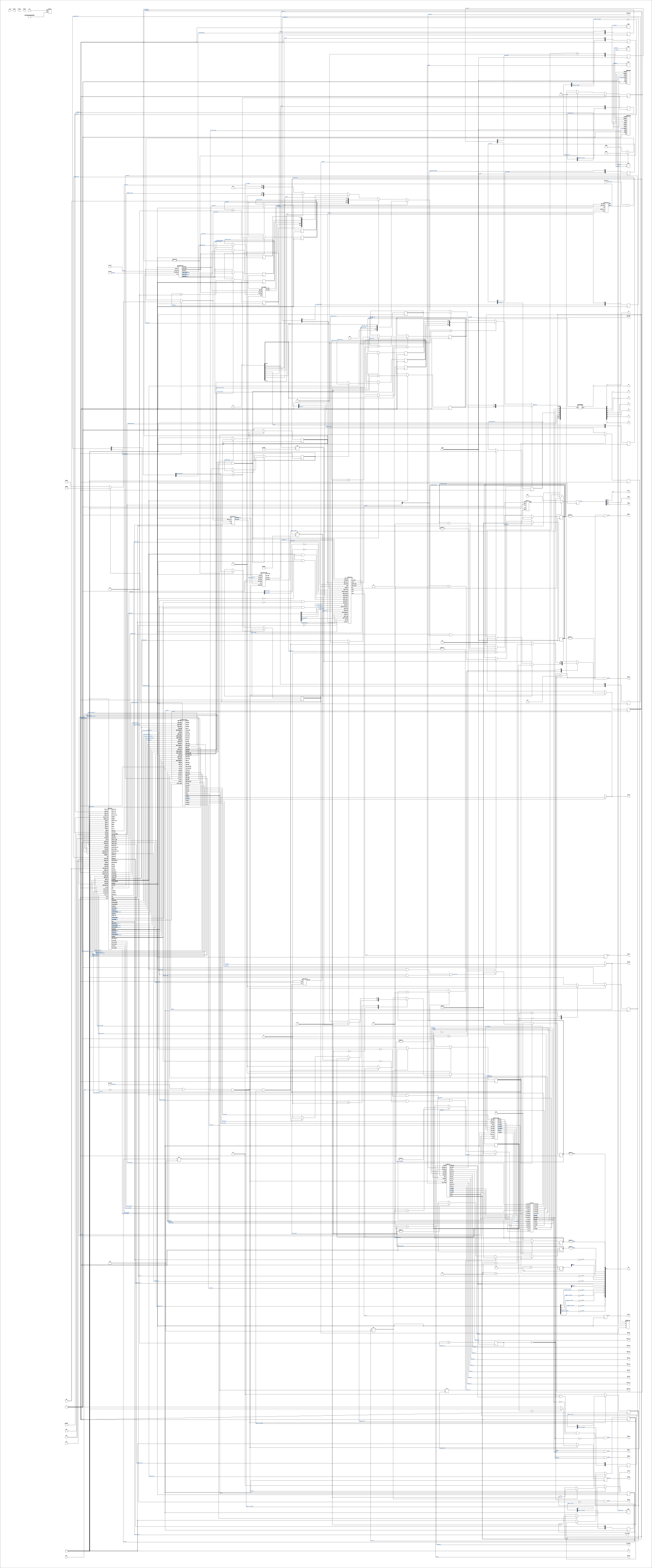
Drawn from the Verilog: the yosys netlist of the Nexys 4 DDR build, where it is the top. Sub-modules are boxes (click the picture to open it full size; there every sub-module box links to its page, and every wire shows its Verilog name).
Description
Nexys 4 DDR / Nexys A7-100T top level for the ND-120 Modelled on the Tang Nano 20K top (fpga/tang-nano-20k/src/ ND120_TANG20K_TOP.v): it instantiates ND120_CORE directly - not ND120_TOP - because the ND-BUS device chain (papertape, floppy, Winchester) only exists on the core, and hangs nd_storage_devices off those seams so the devices are served from real images on the microSD card. DEVICES INCLUDED TAPE-400 papertape at 400 - BOOT.TAP FLOPPY DMA floppy at 1560 - FLOPPY1.IMG / FLOPPY2.IMG WINCHESTER ST506 disc at 500 - WD0.IMG / WD1.IMG (SMD at 1540 is left out - Ronny asked for these three. On the Tang SMD and Winchester are mutually exclusive for want of one BSRAM block; this part has 135 tiles against the Tang's 46, so that constraint does not apply here and SMD could be added later.) STORAGE REGION - CACHED READS, WRITE THROUGH nd_storage's Phase-4 tag directory (SD-FAT/circuit/nd_storage_cache.v) uses a 4 MB region as a CACHE of arbitrarily large images: the disc classes are cached, tape and floppy go direct to the card, and writes go through to the card. Same behaviour as the Tang. WHERE the region lives is the board difference. The Tang has one SDRAM chip shared with CPU main memory, so its region is reached through MEM_RAM_49_SDRAM's ND_STORAGE_PORT. Here main memory is BRAM and the DDR2 is otherwise unused, so the region connects straight to ddr2/nd_ddr2_port.v through ddr2/nd_ddr2_storage.v - no detour through the CPU memory path. When main memory later moves into DDR2, nd_ddr2_port is where the two clients get arbitrated. CLOCKS - one MMCM, VCO 1000 MHz from the 100 MHz oscillator: clk_cpu 1000/60 = 16.667 MHz CPU, bus, OSC and the device chain clk_stor 1000/37 = 27.027 MHz SD/FAT stack, at its proven divisors clk200 1000/5 = 200 MHz the DDR2 controller's input The three are declared asynchronous in build.tcl; every crossing is a two-flop synchroniser or a toggle handshake. MAIN MEMORY is DDR2 with a BRAM cache in front (MAIN_RAM_DDR2, default since 25-AUG-2026): MEM_RAM_49_DDR2 inside MEM_43 reaches the MIG through nd_ddr2_arb, sharing it with the storage region. The old BRAM-only configuration is kept behind build.tcl -tclargs bramram. Build: vivado -mode batch -source build.tcl (see README.md) Last reviewed: 20-AUG-2026 Ronny Hansen
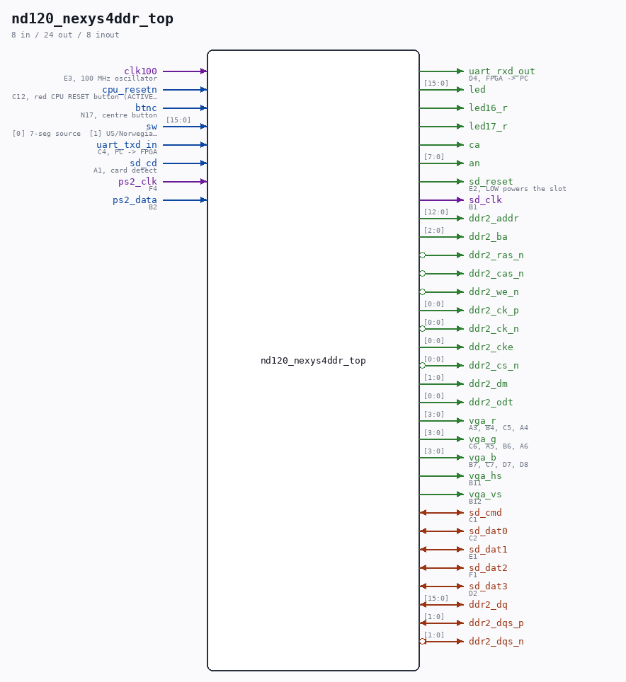
Ports
| Direction | Width | Name | Description |
|---|---|---|---|
| input | 1 |
clk100 |
E3, 100 MHz oscillator |
| input | 1 |
cpu_resetn |
C12, red CPU RESET button (ACTIVE LOW) |
| input | 1 |
btnc |
N17, centre button |
| input | [15:0] |
sw |
[0] 7-seg source [1] US/Norwegian [3] operator panel [4] cache OFF [7] console 9600 baud |
| input | 1 |
uart_txd_in |
C4, PC -> FPGA |
| output | 1 |
uart_rxd_out |
D4, FPGA -> PC |
| output | [15:0] |
led |
|
| output | 1 |
led16_r |
|
| output | 1 |
led17_r |
|
| output | 1 |
ca |
|
| output | [7:0] |
an |
|
| output | 1 |
sd_reset |
E2, LOW powers the slot |
| input | 1 |
sd_cd |
A1, card detect |
| output | 1 |
sd_clk |
B1 |
| inout | 1 |
sd_cmd |
C1 |
| inout | 1 |
sd_dat0 |
C2 |
| inout | 1 |
sd_dat1 |
E1 |
| inout | 1 |
sd_dat2 |
F1 |
| inout | 1 |
sd_dat3 |
D2 |
| inout | [15:0] |
ddr2_dq |
|
| inout | [1:0] |
ddr2_dqs_p |
|
| inout | [1:0] |
ddr2_dqs_n (active low) |
|
| output | [12:0] |
ddr2_addr |
|
| output | [2:0] |
ddr2_ba |
|
| output | 1 |
ddr2_ras_n (active low) |
|
| output | 1 |
ddr2_cas_n (active low) |
|
| output | 1 |
ddr2_we_n (active low) |
|
| output | [0:0] |
ddr2_ck_p |
|
| output | [0:0] |
ddr2_ck_n (active low) |
|
| output | [0:0] |
ddr2_cke |
|
| output | [0:0] |
ddr2_cs_n (active low) |
|
| output | [1:0] |
ddr2_dm |
|
| output | [0:0] |
ddr2_odt |
|
| output | [3:0] |
vga_r |
A3, B4, C5, A4 |
| output | [3:0] |
vga_g |
C6, A5, B6, A6 |
| output | [3:0] |
vga_b |
B7, C7, D7, D8 |
| output | 1 |
vga_hs |
B11 |
| output | 1 |
vga_vs |
B12 |
| input | 1 |
ps2_clk |
F4 |
| input | 1 |
ps2_data |
B2 |
Verilog source
Verilog/fpga/nexys4ddr/nd120_nexys4ddr_top.v on GitHub.
Show the Verilog of nd120_nexys4ddr_top (1595 lines)
/****************************************************************************
** Nexys 4 DDR / Nexys A7-100T top level for the ND-120 **
** **
** Modelled on the Tang Nano 20K top (fpga/tang-nano-20k/src/ **
** ND120_TANG20K_TOP.v): it instantiates ND120_CORE directly - not **
** ND120_TOP - because the ND-BUS device chain (papertape, floppy, **
** Winchester) only exists on the core, and hangs nd_storage_devices off **
** those seams so the devices are served from real images on the microSD **
** card. **
** **
** DEVICES INCLUDED **
** TAPE-400 papertape at 400 - BOOT.TAP **
** FLOPPY DMA floppy at 1560 - FLOPPY1.IMG / FLOPPY2.IMG **
** WINCHESTER ST506 disc at 500 - WD0.IMG / WD1.IMG **
** (SMD at 1540 is left out - Ronny asked for these three. On the Tang **
** SMD and Winchester are mutually exclusive for want of one BSRAM **
** block; this part has 135 tiles against the Tang's 46, so that **
** constraint does not apply here and SMD could be added later.) **
** **
** STORAGE REGION - CACHED READS, WRITE THROUGH **
** nd_storage's Phase-4 tag directory (SD-FAT/circuit/nd_storage_cache.v) **
** uses a 4 MB region as a CACHE of arbitrarily large images: the disc **
** classes are cached, tape and floppy go direct to the card, and writes **
** go through to the card. Same behaviour as the Tang. **
** **
** WHERE the region lives is the board difference. The Tang has one SDRAM **
** chip shared with CPU main memory, so its region is reached through **
** MEM_RAM_49_SDRAM's ND_STORAGE_PORT. Here main memory is BRAM and the **
** DDR2 is otherwise unused, so the region connects straight to **
** ddr2/nd_ddr2_port.v through ddr2/nd_ddr2_storage.v - no detour through **
** the CPU memory path. When main memory later moves into DDR2, **
** nd_ddr2_port is where the two clients get arbitrated. **
** **
** CLOCKS - one MMCM, VCO 1000 MHz from the 100 MHz oscillator: **
** clk_cpu 1000/60 = 16.667 MHz CPU, bus, OSC and the device chain **
** clk_stor 1000/37 = 27.027 MHz SD/FAT stack, at its proven divisors **
** clk200 1000/5 = 200 MHz the DDR2 controller's input **
** The three are declared asynchronous in build.tcl; every crossing is a **
** two-flop synchroniser or a toggle handshake. **
** **
** MAIN MEMORY is DDR2 with a BRAM cache in front (MAIN_RAM_DDR2, default **
** since 25-AUG-2026): MEM_RAM_49_DDR2 inside MEM_43 reaches the MIG **
** through nd_ddr2_arb, sharing it with the storage region. The old **
** BRAM-only configuration is kept behind build.tcl -tclargs bramram. **
** **
** Build: vivado -mode batch -source build.tcl (see README.md) **
** **
** Last reviewed: 20-AUG-2026 **
** Ronny Hansen **
*****************************************************************************/
`default_nettype none
module nd120_nexys4ddr_top (
input wire clk100, // E3, 100 MHz oscillator
input wire cpu_resetn, // C12, red CPU RESET button (ACTIVE LOW)
input wire btnc, // N17, centre button
input wire [15:0] sw, // [0] 7-seg source [1] US/Norwegian [3] operator panel [4] cache OFF [7] console 9600 baud
input wire uart_txd_in, // C4, PC -> FPGA
output wire uart_rxd_out, // D4, FPGA -> PC
output wire [15:0] led,
// tri-colour LEDs LD16/LD17 (active high) - DDR2/arbiter health panel,
// see DEBUG-PANEL.md
output wire led16_r, led16_g, led16_b,
output wire led17_r, led17_g, led17_b,
output wire ca, cb, cc, cd, ce, cf, cg, dp,
output wire [ 7:0] an,
// On-board microSD slot
output wire sd_reset, // E2, LOW powers the slot
input wire sd_cd, // A1, card detect
output wire sd_clk, // B1
inout wire sd_cmd, // C1
inout wire sd_dat0, // C2
inout wire sd_dat1, // E1
inout wire sd_dat2, // F1
inout wire sd_dat3, // D2
// DDR2 - the storage region
inout wire [15:0] ddr2_dq,
inout wire [ 1:0] ddr2_dqs_p,
inout wire [ 1:0] ddr2_dqs_n,
output wire [12:0] ddr2_addr,
output wire [ 2:0] ddr2_ba,
output wire ddr2_ras_n,
output wire ddr2_cas_n,
output wire ddr2_we_n,
output wire [ 0:0] ddr2_ck_p,
output wire [ 0:0] ddr2_ck_n,
output wire [ 0:0] ddr2_cke,
output wire [ 0:0] ddr2_cs_n,
output wire [ 1:0] ddr2_dm,
output wire [ 0:0] ddr2_odt
`ifdef ND120_CONSOLE_VGA
,
// ---- Console on the board's own screen and keyboard --------------------
// Only present when ND120_CONSOLE_VGA is defined, so the default build is
// unchanged down to the pin list. Pins and the plan behind them:
// PLAN-vga-console.md; constraints in nd120_nexys4ddr_console_vga.xdc.
output wire [3:0] vga_r, // A3, B4, C5, A4
output wire [3:0] vga_g, // C6, A5, B6, A6
output wire [3:0] vga_b, // B7, C7, D7, D8
output wire vga_hs, // B11
output wire vga_vs, // B12
// The board's onboard microcontroller is the USB host and hands us a
// plain PS/2 pair - "##USB HID (PS/2)" in Nexys-4-DDR-Master.xdc.
// Receive only, so these are inputs and never driven.
input wire ps2_clk, // F4
input wire ps2_data // B2
`endif
);
/**********************************************
* Clocks *
***********************************************/
wire clk_cpu_pre, clk_stor_pre, clk200_pre;
wire clkfb_out, clkfb_in, mmcm_locked;
wire clk_cpu, clk_stor, clk200;
`ifdef ND120_CONSOLE_VGA
wire clk_pix_pre, clk_pix; // 40 MHz - 800x600@60
wire clk_pix2_pre; // 148.4 MHz - 1920x1080@60, into the mux
`endif
`ifndef ND120_N4DDR_MMCM_DIV
`define ND120_N4DDR_MMCM_DIV 60.0
`endif
MMCME2_BASE #(
.BANDWIDTH ("OPTIMIZED"),
.CLKFBOUT_MULT_F (10.0), // VCO = 100 * 10 = 1000 MHz
.CLKIN1_PERIOD (10.0),
.CLKOUT0_DIVIDE_F(`ND120_N4DDR_MMCM_DIV), // CPU / bus
.CLKOUT1_DIVIDE (37), // 27.027 MHz - SD/FAT stack
.CLKOUT2_DIVIDE (5), // 200 MHz - DDR2 controller
`ifdef ND120_CONSOLE_VGA
// 1000 / 25 = 40.000 MHz EXACTLY - the 800x600@60 pixel clock. No
// fractional divide, no tolerance argument. (640x480 wants 25.175 MHz,
// which this VCO cannot make: the nearest is 25.000, 0.7% low.)
.CLKOUT3_DIVIDE (25), // 40 MHz - VGA console pixel clock
`endif
.DIVCLK_DIVIDE (1),
.STARTUP_WAIT ("FALSE")
) mmcm (
.CLKIN1 (clk100),
.CLKFBIN (clkfb_in),
.CLKFBOUT(clkfb_out),
.CLKOUT0 (clk_cpu_pre),
.CLKOUT1 (clk_stor_pre),
.CLKOUT2 (clk200_pre),
`ifdef ND120_CONSOLE_VGA
.CLKOUT3 (clk_pix_pre),
`endif
.LOCKED (mmcm_locked),
.PWRDWN (1'b0),
.RST (1'b0)
);
BUFG bufg_fb (.I(clkfb_out), .O(clkfb_in));
BUFG bufg_cpu (.I(clk_cpu_pre), .O(clk_cpu));
BUFG bufg_st (.I(clk_stor_pre), .O(clk_stor));
// MIG's project sets SystemClock = "No Buffer", so this must arrive buffered
BUFG bufg_200 (.I(clk200_pre), .O(clk200));
`ifdef ND120_CONSOLE_VGA
// ------------------------------------------------------------------------
// The second pixel clock, and the glitchless mux between them
//
// 1920x1080@60 wants 148.5 MHz, which the main MMCM's 1000 MHz VCO cannot
// divide to (1000/6.73). So the high mode gets its own MMCM:
//
// 100 MHz x 11.875 = 1187.5 MHz VCO, / 8 = 148.4375 MHz
//
// 148.4375 is 0.042% below the nominal 148.5 - far inside what a monitor
// tolerates, and the alternative would be a fractional CLKOUT this part
// cannot produce on anything but CLKOUT0. The VCO sits near the top of the
// -1 speed grade's 600-1200 MHz range; if a future rebuild fails to lock,
// this is the first thing to look at.
//
// BUFGMUX_CTRL, not a plain mux: switching a clock with logic produces runt
// pulses, and a runt pulse on the pixel clock does not give you a glitchy
// picture - it gives you flip-flops that latch garbage in the character RAM.
// The primitive waits for a low phase on both clocks before it changes over.
// ------------------------------------------------------------------------
wire mmcm2_locked, clkfb2_out, clkfb2_in;
MMCME2_BASE #(
.BANDWIDTH ("OPTIMIZED"),
.CLKFBOUT_MULT_F (11.875), // VCO = 100 * 11.875 = 1187.5 MHz
.CLKIN1_PERIOD (10.0),
.CLKOUT0_DIVIDE_F(8.5), // 139.706 MHz - 1080p CVT reduced blanking
.DIVCLK_DIVIDE (1),
.STARTUP_WAIT ("FALSE")
) mmcm_video (
.CLKIN1 (clk100),
.CLKFBIN (clkfb2_in),
.CLKFBOUT(clkfb2_out),
.CLKOUT0 (clk_pix2_pre),
.LOCKED (mmcm2_locked),
.PWRDWN (1'b0),
.RST (1'b0)
);
BUFG bufg_fb2 (.I(clkfb2_out), .O(clkfb2_in));
//! NO BUFG on either clock before the mux, and that is not an oversight.
//! BUFGMUX_CTRL *is* a BUFGCTRL - a global buffer - so putting an ordinary
//! BUFG in front of it cascades two of them, and Vivado will only place that
//! if the two sites happen to be cyclically adjacent in the same half of the
//! SLR. They were not, and placement failed outright:
//!
//! Clock Rule: rule_cascaded_bufg ... Status: FAILED
//! ERROR: [Place 30-99] Placer failed with error: 'IO Clock Placer failed'
//!
//! An MMCM output drives a BUFGCTRL directly on a dedicated route, which is
//! both legal and the intended path. The buffering happens in the mux.
//! sw[2] = 0 : 800x600 at 40 MHz sw[2] = 1 : 1920x1080 at 148.4 MHz
//!
//! The mode bit and the clock MUST change together - the timing generator
//! only counts, it has no way to know what the clock actually is. They are
//! driven from this one net for exactly that reason.
//! sw[2] MUST be debounced before it reaches a clock mux.
//!
//! It was wired straight to the select, unlike sw[1] and sw[3] which are
//! synchronised - an oversight, and a highly visible one. A slide switch has
//! no debounce of its own, so every bounce and every bit of picked-up noise
//! made BUFGMUX_CTRL change the pixel clock between 40 MHz and 139.7 MHz.
//! On screen that does not look like a switch problem, it looks like the
//! picture itself is unstable - reported from hardware as "flickering, like
//! a bad TV from the 1980s".
//!
//! Two flops to synchronise, then a counter requiring the level to hold
//! steady for 2^20 clocks - about 17 ms at 60 MHz, far longer than any
//! mechanical bounce - before the mux is allowed to move.
reg [1:0] s_vmode_sync = 2'b00;
reg [19:0] s_vmode_cnt = 20'd0;
reg s_vmode_r = 1'b0;
always @(posedge clk_cpu) begin
s_vmode_sync <= {s_vmode_sync[0], sw[2]};
if (s_vmode_sync[1] == s_vmode_r) begin
s_vmode_cnt <= 20'd0;
end else if (&s_vmode_cnt) begin
s_vmode_r <= s_vmode_sync[1];
s_vmode_cnt <= 20'd0;
end else begin
s_vmode_cnt <= s_vmode_cnt + 20'd1;
end
end
BUFGMUX_CTRL bufg_pixmux (
.I0(clk_pix_pre), // 40 MHz straight off the main MMCM
.I1(clk_pix2_pre), // 139.7 MHz straight off the video MMCM
.S (s_vmode_r),
.O (clk_pix)
);
wire s_vmode = s_vmode_r;
`endif
/**********************************************
* Reset *
* Held while either button is down or the *
* MMCM is unlocked, then released after a *
* counter in each domain. *
***********************************************/
wire rst_req_n = cpu_resetn & ~btnc & mmcm_locked;
reg [7:0] por_cpu = 8'd0;
reg sys_rst_n_r = 1'b0;
always @(posedge clk_cpu) begin
if (!rst_req_n) begin
por_cpu <= 8'd0;
sys_rst_n_r <= 1'b0;
end else if (por_cpu != 8'hFF) begin
por_cpu <= por_cpu + 8'd1;
end else begin
sys_rst_n_r <= 1'b1;
end
end
wire sys_rst_n = sys_rst_n_r;
/**********************************************
* Storage reset + SD slot power cycle *
* (fix-sd-card, 26-AUG-2026) *
***********************************************/
// The card itself must be POWER CYCLED, not just our logic reset:
// - After SD-card configuration the on-board microcontroller has used
// the card in SPI mode; a card that entered SPI mode leaves it only
// by a power cycle. The manual's own post-DONE slot power cycle can
// be defeated when the fabric drives SD_RESET low (slot ON) the
// instant configuration completes - measured 26-AUG-2026 as FDISK
// error 3 on every disc op after SD-config, while the same card
// boots everything when the bitstream comes in over JTAG.
// - MACL (master clear, DEBUG_MR_n) must reach the card too, so a
// console MACL gives the machine a disc subsystem in a known state.
// So: on ANY trigger (configuration/POR, CPU RESET/BTNC via rst_req_n,
// or a master-clear pulse) the slot is powered OFF for T_OFF, then ON
// with the storage stack held in reset a further T_SETTLE for the
// card's internal boot, then the stack is released and the mount runs
// its full init+scan against a freshly reset card.
localparam [21:0] SDPWR_T_OFF = 22'd2_702_700; // 100 ms at 27.027 MHz
localparam [21:0] SDPWR_T_SETTLE = 22'd1_351_350; // 50 ms
localparam [1:0] SDPWR_OFF = 2'd0, SDPWR_SETTLE = 2'd1, SDPWR_RUN = 2'd2;
// Two reset lines cross from the CPU domain, 2-FF synced, both active
// low, either one triggers the power cycle:
// DEBUG_MR_n - master clear (console MACL, power-up)
// DEBUG_CLEAR_n - the machine's own SYSTEM CLEAR (CLEAR_n out of the
// IO block, ND3202D sheet: "CLEAR_n=0 during reset ->
// MCL fires, initialising all modules") - the same
// reset a real ND-bus peripheral saw, so the disc
// subsystem resets exactly when the machine does.
wire s_debug_mr_n; // declared here: first use is in this block
wire s_debug_clear_n;
reg [1:0] sdpwr_mr_sync = 2'b11;
reg [1:0] sdpwr_clr_sync = 2'b11;
always @(posedge clk_stor) begin
sdpwr_mr_sync <= {sdpwr_mr_sync[0], s_debug_mr_n};
sdpwr_clr_sync <= {sdpwr_clr_sync[0], s_debug_clear_n};
end
wire sdpwr_trigger_n = sdpwr_mr_sync[1] & sdpwr_clr_sync[1]; // 0 = reset asserted
reg [1:0] sdpwr_state = SDPWR_OFF;
reg [21:0] sdpwr_cnt = 22'd0;
reg sd_pwroff_r = 1'b1; // 1 = slot power OFF (sd_reset high)
reg rst_stor_n_r = 1'b0;
always @(posedge clk_stor) begin
if (!rst_req_n) begin
sdpwr_state <= SDPWR_OFF;
sdpwr_cnt <= 22'd0;
sd_pwroff_r <= 1'b1;
rst_stor_n_r <= 1'b0;
end else begin
case (sdpwr_state)
SDPWR_OFF: begin
sd_pwroff_r <= 1'b1;
rst_stor_n_r <= 1'b0;
if (sdpwr_cnt != SDPWR_T_OFF) sdpwr_cnt <= sdpwr_cnt + 22'd1;
else if (sdpwr_trigger_n) begin
// reset lines released (or never asserted): power back on
sdpwr_cnt <= 22'd0;
sdpwr_state <= SDPWR_SETTLE;
end
// a reset line still low: hold here until it releases
end
SDPWR_SETTLE: begin
sd_pwroff_r <= 1'b0;
rst_stor_n_r <= 1'b0;
if (sdpwr_cnt != SDPWR_T_SETTLE) sdpwr_cnt <= sdpwr_cnt + 22'd1;
else begin
sdpwr_cnt <= 22'd0;
sdpwr_state <= SDPWR_RUN;
end
end
default: begin // SDPWR_RUN
sd_pwroff_r <= 1'b0;
rst_stor_n_r <= 1'b1;
if (!sdpwr_trigger_n) begin
// MACL or system clear: power-cycle the card and re-mount
sdpwr_cnt <= 22'd0;
sdpwr_state <= SDPWR_OFF;
end
end
endcase
end
end
wire rst_stor_n = rst_stor_n_r;
/**********************************************
* ND-BUS tie-offs: no external bus here *
***********************************************/
wire BREQ_n = 1'b1, POWSENSE_n = 1'b1;
wire BINT10_n = 1'b1, BINT11_n = 1'b1, BINT12_n = 1'b1;
wire BINT13_n = 1'b1, BINT15_n = 1'b1;
wire [23:0] BD_23_0_n_IN = 24'hFFFFFF;
wire SEMRQ_n_IN = 1'b1, BINPUT_n_IN = 1'b1, BDAP_n_IN = 1'b1;
wire BDRY_n_IN = 1'b1, BAPR_n_IN = 1'b1;
/**********************************************
* Device seams between the core and storage *
***********************************************/
wire TAPE_BYTE_REQ, TAPE_REWIND;
wire s_tape_byte_valid;
wire [ 7:0] s_tape_byte_data;
wire FDISK_REQ, FDISK_WR, FDISK_DONE, FDISK_ERR, FDBUF_WE;
wire [15:0] FDISK_LSECT, FDBUF_WDATA, FDBUF_RDATA;
wire [ 1:0] FDISK_FORMAT, FDISK_DRIVE;
wire [10:0] FDISK_WORDCOUNT;
wire [ 3:0] FDISK_ERR_CODE, FDISK_MEDIA_FMT;
wire [ 9:0] FDBUF_ADDR;
wire WDISK_START, WDISK_REQ, WDISK_WR, WDISK_DONE, WDISK_ERR, WDBUF_WE;
wire [15:0] WDISK_BLKADDR1, WDISK_BLKADDR2, WDBUF_WDATA, WDBUF_RDATA;
wire [ 2:0] WDISK_UNIT;
wire [10:0] WDISK_WORDCOUNT;
wire [ 3:0] WDISK_ERR_CODE;
wire [ 9:0] WDBUF_ADDR;
// SMD is not built into this bitstream; its seam is tied inactive
wire SDISK_START, SDISK_REQ, SDISK_WR;
wire [15:0] SDISK_BLKADDR1, SDISK_BLKADDR2, SDBUF_RDATA;
wire [ 2:0] SDISK_UNIT;
wire [10:0] SDISK_WORDCOUNT;
/**********************************************
* Status / debug *
***********************************************/
wire [ 6:0] s_cpu_led;
wire s_run;
wire [12:0] CSA_12_0;
wire [ 3:0] s_pil;
wire [15:0] s_panel_actlv; // the microcode's ACTIVE LEVEL word, via the panel processor
wire [13:0] s_debug_la_23_10;
wire [ 9:0] s_debug_ca_9_0;
wire [ 4:0] s_debug_cc_term;
wire s_debug_mclk, s_debug_lcs_n, s_debug_fetch;
wire s_debug_map_n; // one falling edge per macro instruction (ND3202D)
wire s_debug_cfetch; // one rise per macro instruction (CGA CFETCH) - feeds the MIPS counter
wire [15:0] s_panel_mips; // XX.XX BCD from mips_counter, once a second
wire s_debug_refrq_n;
wire s_debug_intrq_n, s_debug_powfail_n;
wire [15:0] s_debug_fidbo, s_ireq_15_0_n, s_xmic_dbg;
// PT-write-during-freeze probe. Declared HERE, at module scope with the other
// debug nets, and not inside any `ifdef - see the long note above the DDR2
// port connection. s_dbg_ptw_lvl is driven by the DDR2 main-RAM client and
// r_ptwhold_sticky is read by the 7-segment panel, which every build has.
wire s_dbg_ptw_lvl;
//! Operator-panel status off the CPU board, in MC68705 Port-D order:
//! [1:0] PCR protect ring [2] PONI [3] IONI [4] HIT [5] LEV0
//! Declared here at module scope, above every use, for the same reason the
//! PT-write probe signals now are.
wire [7:0] s_dbg_panel;
//! Cache-write gating bus. Read by the ILA only - see CPU_MMU_24.v's
//! DBG_CACHE port comment for the bit layout and why it was added.
wire [7:0] s_dbg_cache;
reg r_ptwhold_sticky = 1'b0;
reg [15:0] r_ptwhold_cnt = 16'd0;
`ifdef ND120_ILA_MARK_DEBUG
(* mark_debug = "true" *) // keep the name for the ILA (build.tcl ila flag)
`endif
wire cpu_txd;
wire [15:0] DMA_RDATA;
wire DMA_ACK, DMA_ERR, DMA_BUSY;
`ifdef ND120_ERRFA_PROBE
// ERRFA evidence probe (MEM_RAM_49_BLOCKRAM) + the WD-IOX ring: both
// TX lines wire-ANDed onto the console - all idle high; after the
// SINTRAN halt only the probes talk, in disjoint time slots
// (P line ~0.5 s, EF line ~2.0 s, W line ~2.2 s after the crash text).
wire s_errfa_txd, s_wdiox_txd;
wire [15:0] s_efp_iox_addr, s_efp_iox_wdata, s_efp_iox_rdata;
wire s_efp_iox_rd, s_efp_iox_wr;
nd120_errfa_wdiox_ring WDIOX_RING (
.clk(clk_cpu),
.rst_n(sys_rst_n),
.iox_addr(s_efp_iox_addr),
.iox_rd(s_efp_iox_rd),
.iox_wr(s_efp_iox_wr),
.iox_wdata(s_efp_iox_wdata),
.iox_rdata(s_efp_iox_rdata),
.contx(cpu_txd),
.txd(s_wdiox_txd)
);
assign uart_rxd_out = cpu_txd & s_errfa_txd & s_wdiox_txd;
`else
assign uart_rxd_out = cpu_txd;
`endif
/**********************************************
* Console on the board's own screen+keyboard *
* (ND120_CONSOLE_VGA - PLAN-vga-console.md) *
***********************************************/
`ifdef ND120_CONSOLE_VGA
// Framing. The console UART inside the machine is a SC2661 EPCI, which is
// SOFTWARE PROGRAMMED - baud and framing are set at run time, not fixed in
// RTL, so these must match whatever the machine is actually running.
// console.ps1:17 says the OPCOM console is "7E1 in some configurations;
// the board check is plain 8N1"; the deployed fast builds run 115200.
// Wrong values here look like garbage on screen and nothing else.
`ifndef ND120_CONSOLE_BAUD
`define ND120_CONSOLE_BAUD 115200
`endif
`ifndef ND120_CONSOLE_DATA_BITS
`define ND120_CONSOLE_DATA_BITS 7
`endif
`ifndef ND120_CONSOLE_PARITY
`define ND120_CONSOLE_PARITY 1'b1
`endif
// Reset for the pixel domain, same shape as the CPU one above.
reg [7:0] por_pix = 8'd0;
reg pix_rst_n_r = 1'b0;
always @(posedge clk_pix) begin
if (!rst_req_n) begin
por_pix <= 8'd0;
pix_rst_n_r <= 1'b0;
end else if (por_pix != 8'hFF) begin
por_pix <= por_pix + 8'd1;
end else begin
pix_rst_n_r <= 1'b1;
end
end
wire pix_rst_n = pix_rst_n_r;
// --- keyboard/screen national layout, on a physical switch ---------------
//
// sw[1] = 0 : US ANSI sw[1] = 1 : Norwegian (NS 4551-1)
//
// ONE bit drives BOTH the keyboard table and the font page, deliberately. A
// national variant is not a font choice and not a keyboard choice - it is
// one agreement about what six byte values mean. Letting the two be selected
// separately would allow the state where you type AE and the screen draws
// '[', which looks like a font bug and is not one.
//
// Two flops of synchronizer because a slide switch is asynchronous to every
// clock in the design. No debounce: a bouncing switch changes the glyph page
// for a few microseconds, which is invisible, and the keyboard table is only
// consulted at the instant a key is decoded.
//! sw[3] shows/hides the operator panel. Runtime only: the panel logic is in
//! the bitstream either way, so this costs one LUT and saves screen space,
//! not fabric. Removing it entirely is a build-time choice (leave the
//! terminal sources out), not this switch.
reg [1:0] s_panel_sync = 2'b00;
always @(posedge clk_pix) s_panel_sync <= {s_panel_sync[0], sw[3]};
wire s_panel_en = s_panel_sync[1];
reg [1:0] s_layout_sync = 2'b00;
always @(posedge clk_pix) s_layout_sync <= {s_layout_sync[0], sw[1]};
wire s_layout_no = s_layout_sync[1];
// --- machine -> screen ---------------------------------------------------
// Deserialize the console line the machine is already driving. Tapping the
// byte before serialization would be cleaner, but that means adding a port
// to SC2661_UART - shared RTL used by every board and by the Verilator
// reference. This costs one small module and touches nothing shared.
wire s_con_byte_valid;
wire [7:0] s_con_byte_data;
//! Clocks per bit, chosen with the pixel clock. The console shares the video
//! clock domain, so a compile-time divisor would be right in one video mode
//! and produce garbage in the other.
localparam integer CON_DIV_LO = 40_000_000 / `ND120_CONSOLE_BAUD;
localparam integer CON_DIV_HI = 139_705_882 / `ND120_CONSOLE_BAUD;
//! 9600-baud divisors for the same two pixel clocks, selected by sw[7] (the
//! baud switch) so the on-screen console tracks the SC2661 line speed.
localparam integer CON_DIV_LO_9600 = 40_000_000 / 9600;
localparam integer CON_DIV_HI_9600 = 139_705_882 / 9600;
//! sw[7] synced into the pixel-clock domain (the console runs here).
reg [1:0] s_baud_sync_pix = 2'b00;
always @(posedge clk_pix) s_baud_sync_pix <= {s_baud_sync_pix[0], sw[7]};
wire s_baud9600_pix = s_baud_sync_pix[1];
wire [15:0] s_con_divisor =
s_baud9600_pix ? (s_vmode ? CON_DIV_HI_9600[15:0] : CON_DIV_LO_9600[15:0])
: (s_vmode ? CON_DIV_HI[15:0] : CON_DIV_LO[15:0]);
console_uart_rx #(
.CLK_HZ (40_000_000),
.BAUD (`ND120_CONSOLE_BAUD),
.DATA_BITS(`ND120_CONSOLE_DATA_BITS),
.PARITY (`ND120_CONSOLE_PARITY)
) CONSOLE_RX (
.clk (clk_pix),
.rst_n (pix_rst_n),
.divisor_ovr(s_con_divisor),
.rxd (cpu_txd),
.byte_valid(s_con_byte_valid),
.byte_data (s_con_byte_data)
);
wire s_pixel, s_de, s_bell;
//! Box-charset debug taps (01-SEP-2026, sw[4] - see seg_value mux below):
//! whether the terminal is currently in NDSS6/Box mode, and whether it
//! has EVER seen ESC 6 since power-on - answers "did SINTRAN even send
//! the designation" directly, no software layer to doubt.
wire s_dbg_box_mode, s_dbg_saw_esc6;
wire [2:0] s_colour;
//! Sync straight off the core, before the output register below.
wire s_hs_w, s_vs_w;
// --- the power-on banner -------------------------------------------------
// Prints a self-test message before the machine says anything, then gets out
// of the way for good. It is what turns a blank screen from one useless
// symptom into two useful ones: text but no response means the KEYBOARD is
// at fault, nothing at all means the video path is. Shared with the MiSTer
// and MEGA65 consoles - see Terminals/rtl/term_console_feed.v.
wire s_feed_valid;
wire [7:0] s_feed_data;
wire s_term_ready;
term_console_feed FEED (
.clk (clk_pix),
.rst_n(pix_rst_n),
.cpu_valid(s_con_byte_valid),
.cpu_data (s_con_byte_data),
// Nothing to back-pressure. This byte came off a real serial line that
// has already sent it - there is no way to ask the machine to wait, so
// a byte arriving mid-banner is dropped. That is safe here and not by
// luck: the banner runs for ~1900 pixel clocks (~48 us) immediately
// after reset, which is under one byte time at 115200, and the CPU is
// still in reset for all of it.
.cpu_ready(),
// No local echo on this board: the ND-120 echoes what you type, and a
// terminal that echoes as well shows every character twice.
.echo_valid(1'b0),
.echo_data (8'h00),
.term_valid(s_feed_valid),
.term_data (s_feed_data),
.term_ready(s_term_ready),
.banner_done()
);
terminal_top #(
.FONT_FILE("font8x16.hex"), // Vivado resolves $readmemh next to the .v
// TDV2200 is 80x25 (the status-line row PED uses), VT100 is 80x24 -
// see terminal_ctrl_tdv.v's header. Must track the same
// ND120_TERMINAL_VT100 define the controller selection uses below.
`ifdef ND120_TERMINAL_VT100
.ROWS(24)
`else
.ROWS(25)
`endif
) TERMINAL (
// The deserializer already runs on the pixel clock, so the crossing
// inside terminal_top is a no-op here. Left in place rather than
// bypassed: it is what makes the core drop onto MiSTer and the MEGA65
// unchanged, and it costs three flops.
.byte_clk (clk_pix),
.byte_rst_n(pix_rst_n),
.byte_valid(s_feed_valid),
.byte_data (s_feed_data),
.byte_ready(s_term_ready),
.national (s_layout_no),
.mode (s_vmode),
// Operator panel. Signals come straight off ND3202D's DBG_PANEL port,
// which is the SAME five the real MC68705 panel processor samples on its
// Port D - see the port comment in ND3202D.v.
// [1:0] PCR [2] PONI [3] IONI [4] LHIT [5] LEV0
.panel_enable (s_panel_en),
.panel_pil (s_pil),
.panel_actlv (s_panel_actlv),
// CPU board lamps: LED[0] RED (MACL in progress), LED[1] GREEN
// (initialisation complete - only written once the self-test passes).
// INVERTED: active low at the source - IO_REG_41.v:145-148 drives
// these from s_emcl_n / s_led3_green_n, both marked "active low".
// INVERTED, and that is MEASURED, not deduced. Both signals are ACTIVE
// LOW at the source (IO_REG_41.v drives IOLED[0] from s_emcl_n and
// IOLED[1] from s_led3_green_n), and term_panel lights a lamp on 1.
// The MiSTer port measured this on 31-AUG-2026: "passing them straight
// through showed every lamp backwards", and GREEN lights correctly
// there with these inversions in place (fpga/mister/nd120.sv:511-518).
//
// I removed these on 01-SEP on the strength of the IOC register
// comments ("red LED ON1", "green LED on1") reading as active-high.
// That was wrong: it overrode an existing hardware measurement with an
// interpretation of an ambiguous comment. Do not remove them again
// without a fresh measurement that contradicts MiSTer's.
.panel_cpu_red (~s_cpu_led[0]),
.panel_cpu_green (~s_cpu_led[1]),
.panel_lev0 (s_dbg_panel[5]),
// [4] is LHIT - the same signal the real MC68705 panel samples, not the
// cache's raw comparator output. [6] (LAPA_n) is no longer read here:
// the rate comes from LHIT over time, so there is no denominator.
.panel_hit (s_dbg_panel[4]),
.panel_ring (s_dbg_panel[1:0]),
.panel_paging_on (s_dbg_panel[2]),
.panel_interrupt_on(s_dbg_panel[3]),
// RUN_n is active LOW on this board - "low while CPU is running", which
// is what drives the real front-panel RUN lamp.
.panel_running (~s_run),
// Disc activity. REQ with WR low is a read, WR high a write - the same
// decode the board's activity LEDs already use a few hundred lines down.
.panel_hdd_rd (WDISK_REQ & ~WDISK_WR),
.panel_hdd_wr (WDISK_REQ & WDISK_WR),
.panel_flp_rd (FDISK_REQ & ~FDISK_WR),
.panel_flp_wr (FDISK_REQ & FDISK_WR),
// MIPS - counted from the board FETCH signal on the CPU clock, four
// BCD digits once a second. See mips_counter.v; crossing is inside
// terminal_top, same as ACTLV.
.panel_mips (s_panel_mips),
.colour (s_colour),
.pix_clk (clk_pix),
.pix_rst_n(pix_rst_n),
.pixel (s_pixel),
.hsync (s_hs_w),
.vsync (s_vs_w),
.de (s_de),
.bell (s_bell),
.dbg_box_mode(s_dbg_box_mode),
.dbg_saw_esc6(s_dbg_saw_esc6)
);
// The terminal core says WHICH of eight things this pixel is; the board picks
// the actual colour, because colour depth is a board property. The console
// text stays green - this is a 1988 minicomputer and the Tandberg terminals
// it grew up with were green - and the panel colours are sampled from the
// photograph of the real folio panel, not chosen:
//
// fascia #191b19 LCD ground #b6c2a4 LCD segment #2a3226
// silkscreen #d6d9d2 lit legend #e04a63 (measured red, NOT amber)
reg [11:0] s_rgb;
always @(*) begin
case (s_colour)
3'd0: s_rgb = 12'h000; // black
3'd1: s_rgb = 12'h0F0; // console text, green
3'd2: s_rgb = 12'h111; // panel fascia
3'd3: s_rgb = 12'hDDD; // silkscreen label
3'd4: s_rgb = 12'hBCA; // LCD ground
3'd5: s_rgb = 12'h232; // LCD segment
3'd6: s_rgb = 12'hE46; // lit legend
3'd7: s_rgb = 12'h444; // unlit legend
default: s_rgb = 12'h000;
endcase
end
//! REGISTERED on the way out, not driven combinationally from the palette
//! lookup. A combinational path to a pin carries every intermediate value the
//! logic passes through on the way to its answer, and into a resistor-ladder
//! DAC those are real analogue steps - narrow, but the monitor samples
//! continuously, so they show as shimmer on edges. One flop costs one pixel
//! of delay and gives the DAC a single clean transition per pixel. Sync goes
//! through the same stage so it stays aligned with the colour.
reg [11:0] s_rgb_q;
reg s_hs_q, s_vs_q;
always @(posedge clk_pix) begin
s_rgb_q <= s_de ? s_rgb : 12'h000;
s_hs_q <= s_hs_w;
s_vs_q <= s_vs_w;
end
assign vga_hs = s_hs_q;
assign vga_vs = s_vs_q;
assign vga_r = s_rgb_q[11:8];
assign vga_g = s_rgb_q[7:4];
assign vga_b = s_rgb_q[3:0];
// --- keyboard -> machine -------------------------------------------------
wire s_key_valid;
wire [7:0] s_key_data;
//! Raw-scancode debug tap (01-SEP-2026): the Up arrow was reported dead
//! on real hardware while Down/Left/Right/PageUp all work, and static RTL
//! review of the identically-shaped table entries found nothing - so this
//! latches the actual PS/2 byte for eyeball verification on the 7-seg
//! display (sw[5], see the seg_value mux below) instead of trusting
//! another layer of software to report it faithfully.
//! r_dbg_seq (01-SEP-2026): a plain last-value latch cannot tell a real
//! repeat of the same byte from a dead key that never fired at all - the
//! display would just show whatever the PREVIOUS real keypress was
//! forever. This 4-bit counter increments on every code_valid, so the
//! leading digit visibly moves on a genuine new event; if it does NOT
//! move when a key is pressed, that key sent nothing.
wire s_dbg_code_valid;
wire [7:0] s_dbg_code_data;
wire s_dbg_code_release;
wire s_dbg_code_extended;
reg [3:0] r_dbg_seq = 4'h0;
reg [7:0] r_dbg_last_code = 8'h00;
reg r_dbg_last_release = 1'b0;
reg r_dbg_last_extended = 1'b0;
always @(posedge clk_pix) begin
if (s_dbg_code_valid) begin
r_dbg_seq <= r_dbg_seq + 4'h1;
r_dbg_last_code <= s_dbg_code_data;
r_dbg_last_release <= s_dbg_code_release;
r_dbg_last_extended <= s_dbg_code_extended;
end
end
//! Decoded-byte debug tap (01-SEP-2026, sw[6]): F1/F2 confirmed correct
//! RAW scancodes (0x05/0x06) but were reported as doing nothing - the
//! raw-scancode tap above only proves the keyboard and the receiver are
//! right, not that ps2_ascii_table_tdv.v's marker or key_tdv2200.v's
//! ESC[nn_ expansion are. This latches s_key_valid/s_key_data (the
//! ps2_keyboard_tdv output that FEEDS key_tdv2200.v) the same way, so a
//! marker byte (0x80|n, e.g. 0xB2 for F1's ESC[50_) is directly visible.
reg [3:0] r_dbg_seq2 = 4'h0;
reg [7:0] r_dbg_last_ascii = 8'h00;
always @(posedge clk_pix) begin
if (s_key_valid) begin
r_dbg_seq2 <= r_dbg_seq2 + 4'h1;
r_dbg_last_ascii <= s_key_data;
end
end
// Same VT100/TDV2200 compile-time select as the display side - see
// terminal_top.v's CTRL instantiation. ps2_keyboard/key_vt100 and
// ps2_keyboard_tdv/key_tdv2200 are genuinely separate module pairs (the
// PS/2 framing and the sequence-expander FIFO are near-identical, but the
// scancode table and the wire format they expand to are not), never both
// in the same build.
`ifdef ND120_TERMINAL_VT100
ps2_keyboard KEYBOARD (
`else
ps2_keyboard_tdv KEYBOARD (
`endif
.clk (clk_pix),
.rst_n(pix_rst_n),
.ps2_clk_in (ps2_clk),
.ps2_data_in(ps2_data),
.layout_no (s_layout_no),
.ascii_valid(s_key_valid),
.ascii_data (s_key_data),
// raw scancodes: latched above for the 7-seg debug tap, sw[5]
.code_valid (s_dbg_code_valid),
.code_data (s_dbg_code_data),
.code_release (s_dbg_code_release),
.code_extended(s_dbg_code_extended)
);
wire s_kbd_txd;
//! Sequence expander: a TDV F-key or a VT100 arrow is several bytes on
//! the wire (ESC [ ...), and the UART needs ~870 us per byte - so this
//! carries the FIFO that used to be "a problem nobody has". Plain
//! characters pass straight through it either way.
wire s_seq_valid;
wire [7:0] s_seq_data;
wire s_tx_ready;
`ifdef ND120_TERMINAL_VT100
key_vt100 KEYEXP (
`else
key_tdv2200 KEYEXP (
`endif
.clk (clk_pix),
.rst_n (pix_rst_n),
.key_valid(s_key_valid),
.key_data (s_key_data),
.out_valid(s_seq_valid),
.out_data (s_seq_data),
.out_ready(s_tx_ready)
);
console_uart_tx #(
.CLK_HZ (40_000_000),
.BAUD (`ND120_CONSOLE_BAUD),
.DATA_BITS (`ND120_CONSOLE_DATA_BITS),
.PARITY (`ND120_CONSOLE_PARITY),
.PARITY_ODD(1'b0)
) CONSOLE_TX (
.divisor_ovr(s_con_divisor),
.clk (clk_pix),
.rst_n (pix_rst_n),
.byte_valid(s_seq_valid),
.byte_data (s_seq_data),
.ready (s_tx_ready),
.txd (s_kbd_txd)
);
// Both lines idle HIGH, so ANDing merges them - the same idiom this file
// already uses outbound (uart_rxd_out above). The PC console keeps working
// exactly as before; the two only collide if somebody types on the keyboard
// at the instant the PC sends a character.
wire s_console_rxd = uart_txd_in & s_kbd_txd;
`else
wire s_console_rxd = uart_txd_in;
`endif
/**********************************************
* The ND-120 core with its device chain *
***********************************************/
//! sw[4] = the ND-100 console's cache switch (SW1 on the real console,
//! sheet 25 CON). DOWN (0) = cache ON - the state every image deployed
//! since 28-AUG-2026 had - UP (1) = cache OFF, every access to main memory,
//! CSR reports the cache disabled. A runtime switch so the cache can be
//! compared A/B on one bitstream (Ronny, 29-AUG-2026); -tclargs nocache
//! still compiles the cache RAMs out entirely. Two flops on clk_cpu: the
//! switch is a plain slide switch on another domain. Flipping it while
//! SINTRAN runs is the same as throwing the real switch on a running
//! machine - allowed by the hardware, but the cache contents are not
//! flushed by it, so do it at the OPCOM prompt or reboot afterwards.
reg [1:0] s_cache_sw_sync = 2'b00;
always @(posedge clk_cpu) s_cache_sw_sync <= {s_cache_sw_sync[0], sw[4]};
//! sw[7] = console baud select (UP = 9600, DOWN = 115200), synced to the CPU
//! clock for the SC2661 divisor. The on-screen terminal tracks it via
//! s_baud9600_pix above. Software that cannot take 115200 runs at 9600 with
//! no rebuild; the microcode baud thumbwheel stays at 9600 so boot is
//! unaffected - only the physical SC2661 divisor changes.
reg [1:0] s_baud_sync_cpu = 2'b00;
always @(posedge clk_cpu) s_baud_sync_cpu <= {s_baud_sync_cpu[0], sw[7]};
wire s_baud9600_cpu = s_baud_sync_cpu[1];
wire s_cache_on = ~s_cache_sw_sync[1];
ND120_CORE #(
.INCLUDE_TAPE (1),
.INCLUDE_FLOPPY(1),
.INCLUDE_SMD (0),
.INCLUDE_WD (1)
) CORE (
.BAUD_9600(s_baud9600_cpu), // sw[7]: console 9600 (else 115200)
`ifdef ND120_ERRFA_PROBE
.ERRFA_CONTX(cpu_txd),
.ERRFA_TXD(s_errfa_txd),
.ERRFA_IOX_ADDR(s_efp_iox_addr),
.ERRFA_IOX_RD(s_efp_iox_rd),
.ERRFA_IOX_WR(s_efp_iox_wr),
.ERRFA_IOX_WDATA(s_efp_iox_wdata),
.ERRFA_IOX_RDATA(s_efp_iox_rdata),
`endif
.clk_cpu (clk_cpu),
.sys_rst_n(sys_rst_n),
.CACHE_SW (s_cache_on), // console SW1 from slide switch sw[4], see above
.BREQ_n (BREQ_n),
.BINT10_n (BINT10_n),
.BINT11_n (BINT11_n),
.BINT12_n (BINT12_n),
.BINT13_n (BINT13_n),
.BINT15_n (BINT15_n),
.POWSENSE_n (POWSENSE_n),
.BD_23_0_n_IN (BD_23_0_n_IN),
.BD_23_0_n_OUT(),
.SEMRQ_n_IN (SEMRQ_n_IN),
.SEMRQ_n_OUT (),
.BINPUT_n_IN (BINPUT_n_IN),
.BINPUT_n_OUT (),
.BDAP_n_IN (BDAP_n_IN),
.BDAP_n_OUT (),
.BDRY_n_IN (BDRY_n_IN),
.BDRY_n_OUT (),
.BAPR_n_IN (BAPR_n_IN),
.BAPR_n_OUT (),
.BREF_n (),
.BERROR_n (),
.BINACK_n (),
.BIOXE_n (),
.BMEM_n (),
.OUTGRANT_n (),
.OUTIDENT_n (),
.MCL (),
// s_console_rxd is the PC line alone by default, or the PC line ANDed
// with the local keyboard when ND120_CONSOLE_VGA is defined.
.RXD(s_console_rxd),
.TXD(cpu_txd),
.TAPE_BYTE_REQ (TAPE_BYTE_REQ),
.TAPE_BYTE_VALID(s_tape_byte_valid),
.TAPE_BYTE_DATA (s_tape_byte_data),
.TAPE_REWIND (TAPE_REWIND),
.DMA_REQ (1'b0),
.DMA_WR (1'b0),
.DMA_ADDR (24'd0),
.DMA_WDATA(16'd0),
.DMA_RDATA(DMA_RDATA),
.DMA_ACK (DMA_ACK),
.DMA_ERR (DMA_ERR),
.DMA_BUSY (DMA_BUSY),
.FDISK_REQ (FDISK_REQ),
.FDISK_WR (FDISK_WR),
.FDISK_LSECT (FDISK_LSECT),
.FDISK_FORMAT (FDISK_FORMAT),
.FDISK_DRIVE (FDISK_DRIVE),
.FDISK_WORDCOUNT(FDISK_WORDCOUNT),
.FDISK_DONE (FDISK_DONE),
.FDISK_ERR (FDISK_ERR),
.FDISK_ERR_CODE (FDISK_ERR_CODE),
.FDISK_MEDIA_FMT(FDISK_MEDIA_FMT),
.FDBUF_ADDR (FDBUF_ADDR),
.FDBUF_WDATA (FDBUF_WDATA),
.FDBUF_WE (FDBUF_WE),
.FDBUF_RDATA (FDBUF_RDATA),
// SMD absent from this build: outputs left open, inputs inactive
.SDISK_START (SDISK_START),
.SDISK_REQ (SDISK_REQ),
.SDISK_WR (SDISK_WR),
.SDISK_BLKADDR1 (SDISK_BLKADDR1),
.SDISK_BLKADDR2 (SDISK_BLKADDR2),
.SDISK_UNIT (SDISK_UNIT),
.SDISK_WORDCOUNT(SDISK_WORDCOUNT),
.SDISK_DONE (1'b0),
.SDISK_ERR (1'b0),
.SDISK_ERR_CODE (4'd0),
.SDBUF_ADDR (10'd0),
.SDBUF_WDATA (16'd0),
.SDBUF_WE (1'b0),
.SDBUF_RDATA (SDBUF_RDATA),
.WDISK_START (WDISK_START),
.WDISK_REQ (WDISK_REQ),
.WDISK_WR (WDISK_WR),
.WDISK_BLKADDR1 (WDISK_BLKADDR1),
.WDISK_BLKADDR2 (WDISK_BLKADDR2),
.WDISK_UNIT (WDISK_UNIT),
.WDISK_WORDCOUNT(WDISK_WORDCOUNT),
.WDISK_DONE (WDISK_DONE),
.WDISK_ERR (WDISK_ERR),
.WDISK_ERR_CODE (WDISK_ERR_CODE),
.WDBUF_ADDR (WDBUF_ADDR),
.WDBUF_WDATA (WDBUF_WDATA),
.WDBUF_WE (WDBUF_WE),
.WDBUF_RDATA (WDBUF_RDATA),
.LED (s_cpu_led),
.RUN_n (s_run),
.CSA_12_0 (CSA_12_0),
.PIL (s_pil),
.LA_23_10 (s_debug_la_23_10),
.CA_9_0 (s_debug_ca_9_0),
.DEBUG_CC_TERM (s_debug_cc_term),
.DEBUG_MCLK (s_debug_mclk),
.DEBUG_LCS_n (s_debug_lcs_n),
.DEBUG_FETCH (s_debug_fetch),
.DEBUG_MAP_n (s_debug_map_n),
.DEBUG_CFETCH (s_debug_cfetch),
.DEBUG_MR_n (s_debug_mr_n),
.DEBUG_CLEAR_n (s_debug_clear_n),
.DEBUG_REFRQ_n (s_debug_refrq_n),
.DEBUG_INTRQ_n (s_debug_intrq_n),
.DEBUG_POWFAIL_n (s_debug_powfail_n),
.DEBUG_FIDBO_15_0 (s_debug_fidbo),
.DEBUG_IREQ_15_0_N(s_ireq_15_0_n),
.XMIC_DBG_15_0 (s_xmic_dbg)
// ---------------------------------------------------------------------------
// PT-write-during-freeze probe - DECLARED UNCONDITIONALLY, and that is the
// whole point (fixed 28-AUG-2026).
//
// These three sat inside `ifdef ND120_ILA_MARK_DEBUG` while s_dbg_ptw_lvl is
// used by the DDR2 port connection just below, and r_ptwhold_sticky is used by
// the 7-segment debug panel, which is in no `ifdef` at all. So any build with
// DDR2 main memory and WITHOUT an ILA lost the declarations and kept the uses:
// ERROR: [Synth 8-36] 's_dbg_ptw_lvl' is not declared
// Nobody hit it because every recorded build used an ILA flavour (the timing
// table in README.md says `ilaslim` for every run), so the plain path was
// never synthesized.
//
// This is the SECOND time this exact bug has been fixed here - b958fcc moved
// DBG_PTW_LVL out of the MAIN_RAM_SDRAM port block for the same reason, and it
// landed inside the ILA block instead of at module scope. A debug signal that
// anything outside a conditional touches must be declared outside every
// conditional. The mark_debug wires that only the ILA reads stay inside.
// ---------------------------------------------------------------------------
`ifdef MAIN_RAM_DDR2
,
// main-memory DDR2 client (MEM_RAM_49_DDR2 inside MEM_43) -> nd_ddr2_arb
.ui_clk (ui_clk),
.ui_rst (ui_rst),
.mm_req_valid(mm_req_valid),
.mm_req_we (mm_req_we),
.mm_req_addr (mm_req_addr),
.mm_req_wdata(mm_req_wdata),
.mm_req_wmask(mm_req_wmask),
.mm_req_ready(mm_req_ready),
.mm_rsp_valid(mm_rsp_valid),
.mm_rsp_rdata(mm_rsp_rdata),
.DBG_DDR2_BRIDGE(s_dbg_ddr2_bridge),
.DBG_PTW_LVL (s_dbg_ptw_lvl),
.DBG_PANEL (s_dbg_panel),
.PANEL_ACTLV (s_panel_actlv),
.DBG_CACHE (s_dbg_cache)
`endif
);
// --- MIPS counter --------------------------------------------------------
// Macro instructions per second for the panel. Counted from MAP, not
// FETCH (changed 30-AUG-2026): the microsequencer's MAP operation is the
// last microinstruction of every macro instruction - one falling edge of
// MAP_n per instruction, cache hit or miss. FETCH marks memory CYCLES,
// and build 8 (the first image whose cache really hits) starved it: a
// warm machine fetched from the cache, no memory cycle ran, and the
// panel said 00.00 while SINTRAN was visibly running. The counter takes
// a rising-edge input, so MAP_n goes in inverted.
// The CPU frequency follows the MMCM divisor define, so a -Variant build
// measures itself correctly without another number to keep in sync.
// real->integer localparam rounds at elaboration; every tool here (Vivado,
// Verilator, iverilog) does this, while $rtoi in a parameter position is
// less universally loved.
localparam integer MIPS_CLOCK_HZ = 1000000000.0 / `ND120_N4DDR_MMCM_DIV;
mips_counter #(
.CLOCK_HZ(MIPS_CLOCK_HZ)
) MIPS (
.clk (clk_cpu),
.rst_n (sys_rst_n),
// CFETCH since 30-AUG evening: the CGA's own Command Fetch state,
// once per macro instruction, cache present or not. The FETCH and
// MAP_n taps before it were both memory-cycle signals (see the
// history above) - kept wired for probes, no longer counted.
.fetch (s_debug_cfetch),
.mips_bcd(s_panel_mips)
);
/**********************************************
* Storage: images on the microSD card *
***********************************************/
// The slot's power gate. Reference manual section 12: after configuration
// the on-board microcontroller releases the SD bus and SD_RESET must be
// driven LOW by the FPGA to power the slot. Driven by the power-cycle
// controller above (fix-sd-card): held HIGH (slot OFF) for 100 ms at
// every configuration, reset and master clear, so the card always
// starts from power-on state - never a constant again.
assign sd_reset = sd_pwroff_r;
wire s_sd_clk_o;
wire s_sd_cmd_o, s_sd_cmd_oe;
wire s_sd_dat0_o, s_sd_dat0_oe;
wire [1:0] s_sd_status;
wire mem_start, mem_we, mem_busy, mem_done;
wire [19:0] mem_addr;
wire [31:0] mem_wdata, mem_rdata;
nd_storage_devices #(
.SIMULATE (0),
.INCLUDE_TAPE (1),
.INCLUDE_FLOPPY(1),
.INCLUDE_SMD (0),
.INCLUDE_WD (1),
// 8.3 name: ".BPUN" is a 4-character extension that FAT can only hold
// through a VFAT long-name entry, and the floppy/WD builds strip long-
// name parsing. Same choice the Tang makes.
.BOOT_NAME("BOOT.TAP"),
.BOOT_LEN (8'd8)
) STORAGE (
.clk_stor (clk_stor),
.rst_stor_n(rst_stor_n),
.clk_cpu (clk_cpu),
.rst_cpu_n (sys_rst_n),
.byte_req (TAPE_BYTE_REQ),
.byte_valid (s_tape_byte_valid),
.byte_data (s_tape_byte_data),
.source_rewind (TAPE_REWIND),
.TDISK_FAULT (),
.TDISK_ERR_CODE(),
.FDISK_REQ (FDISK_REQ),
.FDISK_WR (FDISK_WR),
.FDISK_LSECT (FDISK_LSECT),
.FDISK_FORMAT (FDISK_FORMAT),
.FDISK_DRIVE (FDISK_DRIVE),
.FDISK_WORDCOUNT(FDISK_WORDCOUNT),
.FDISK_DONE (FDISK_DONE),
.FDISK_ERR (FDISK_ERR),
.FDISK_ERR_CODE (FDISK_ERR_CODE),
.FDISK_MEDIA_FMT(FDISK_MEDIA_FMT),
.FDBUF_ADDR (FDBUF_ADDR),
.FDBUF_WDATA (FDBUF_WDATA),
.FDBUF_WE (FDBUF_WE),
.FDBUF_RDATA (FDBUF_RDATA),
.SDISK_START (SDISK_START),
.SDISK_REQ (SDISK_REQ),
.SDISK_WR (SDISK_WR),
.SDISK_BLKADDR1 (SDISK_BLKADDR1),
.SDISK_BLKADDR2 (SDISK_BLKADDR2),
.SDISK_UNIT (SDISK_UNIT),
.SDISK_WORDCOUNT(SDISK_WORDCOUNT),
.SDISK_DONE (),
.SDISK_ERR (),
.SDISK_ERR_CODE (),
.SDBUF_ADDR (),
.SDBUF_WDATA (),
.SDBUF_WE (),
.SDBUF_RDATA (SDBUF_RDATA),
.WDISK_START (WDISK_START),
.WDISK_REQ (WDISK_REQ),
.WDISK_WR (WDISK_WR),
.WDISK_BLKADDR1 (WDISK_BLKADDR1),
.WDISK_BLKADDR2 (WDISK_BLKADDR2),
.WDISK_UNIT (WDISK_UNIT),
.WDISK_WORDCOUNT(WDISK_WORDCOUNT),
.WDISK_DONE (WDISK_DONE),
.WDISK_ERR (WDISK_ERR),
.WDISK_ERR_CODE (WDISK_ERR_CODE),
.WDBUF_ADDR (WDBUF_ADDR),
.WDBUF_WDATA (WDBUF_WDATA),
.WDBUF_WE (WDBUF_WE),
.WDBUF_RDATA (WDBUF_RDATA),
.sd_clk_o (s_sd_clk_o),
.sd_cmd_i (sd_cmd),
.sd_cmd_o (s_sd_cmd_o),
.sd_cmd_oe (s_sd_cmd_oe),
.sd_dat0_i (sd_dat0),
.sd_dat0_o (s_sd_dat0_o),
.sd_dat0_oe(s_sd_dat0_oe),
.mem_start(mem_start),
.mem_we (mem_we),
.mem_addr (mem_addr),
.mem_wdata(mem_wdata),
.mem_rdata(mem_rdata),
.mem_busy (mem_busy),
.mem_done (mem_done),
.DBG_STATE (),
.DBG_LBA (),
.DBG_WDATA (),
.DBG_RDATA (),
.DBG_BUFW (),
.DBG_BUFWE (),
.DBG_FSEC (),
.DBG_RX_STB (),
.DBG_RX_RAW (),
.DBG_RX_BYTE (),
.DBG_PAST_EOF(),
.DBG_GRANT (),
.sd_status (s_sd_status)
);
// The ONLY tristate drivers in the design sit here at the pads (repo rule:
// no 'z' inside the fabric). DAT1-3 are parked high: the stack runs 1-bit,
// and DAT3 high at CMD0 is what keeps the card out of SPI mode.
assign sd_clk = s_sd_clk_o;
assign sd_cmd = s_sd_cmd_oe ? s_sd_cmd_o : 1'bz;
assign sd_dat0 = s_sd_dat0_oe ? s_sd_dat0_o : 1'bz;
assign sd_dat1 = 1'bz;
assign sd_dat2 = 1'bz;
assign sd_dat3 = 1'bz;
/**********************************************
* DDR2: main memory (BRAM cache in front, *
* MEM_RAM_49_DDR2 inside the core) and the *
* storage region share the MIG through *
* nd_ddr2_arb. Main memory wins a tie - a *
* frozen CPU cycle is waiting on it. *
***********************************************/
wire ui_clk, ui_rst, calib_done;
wire req_valid, req_we, req_ready, rsp_valid;
wire [ 26:0] req_addr;
wire [127:0] req_wdata, rsp_rdata;
wire [ 15:0] req_wmask;
// client A: main memory (from ND120_CORE / MEM_RAM_49_DDR2)
wire mm_req_valid, mm_req_we, mm_req_ready, mm_rsp_valid;
wire [ 26:0] mm_req_addr;
wire [127:0] mm_req_wdata, mm_rsp_rdata;
wire [ 15:0] mm_req_wmask;
wire [ 7:0] s_dbg_ddr2_bridge;
// Sticky/counter for the PT-write-during-freeze probe. Unconditional: the
// sticky bit is shown on the 7-segment panel in every build. See the long
// note above the DDR2 port connection for why this is not inside the ILA
// ifdef where it used to live.
always @(posedge clk_cpu) begin
if (s_dbg_ptw_lvl & s_dbg_ddr2_bridge[4]) begin
r_ptwhold_sticky <= 1'b1;
r_ptwhold_cnt <= r_ptwhold_cnt + 16'd1;
end
end
`ifdef ND120_ILA_MARK_DEBUG
// ilaslim (build.tcl): DDR2 main-RAM bridge state next to CSA/cpu_txd.
// [7:5] astate [4] MEM_HOLD [3] last_hit [2] refill_pend
// [1] op_busy [0] have_data
(* mark_debug = "true" *) wire [7:0] s_ila_ddr2 = s_dbg_ddr2_bridge;
// PT-write-during-freeze overlap probe (27-AUG, wrong-PPN option 1).
// DBG_PTW_LVL = the LIVE ~EPT_n & ~WMAP_n strobe conjunction out of
// CPU_MMU_24; bridge[4] = MEM_HOLD. Sticky + cycle counter: if the sticky
// never sets across a boot, a PT write NEVER overlaps a DDR2 freeze and
// the write-during-freeze corruption hypothesis is dead; if it sets, the
// counter says how many overlap cycles, and the ILA nets let a capture
// look at what moved during the window.
(* mark_debug = "true" *) wire s_ila_ptwhold_stk = r_ptwhold_sticky;
(* mark_debug = "true" *) wire [15:0] s_ila_ptwhold_cnt = r_ptwhold_cnt;
(* mark_debug = "true" *) wire s_ila_ptwhold_lvl = s_dbg_ptw_lvl;
// 25-AUG SINTRAN-hang hunt: the CPU loops at CSA 0o6000 (the execute-zeros
// signature) - capture WHERE it fetches from and the microsequencer state.
(* mark_debug = "true" *) wire [13:0] s_ila_la = s_debug_la_23_10;
(* mark_debug = "true" *) wire [15:0] s_ila_xmic = s_xmic_dbg;
// interrupt-subsystem view for the idle-loop diagnosis: current level and
// the raw request vector into the controller (PIE/PID themselves are
// serviced constructs inside CGA_INTR, not plain registers)
//! The cache-write gating bus. WCA_n is the one that matters: if it never
//! goes low the cache is never written, which is exactly what CACHE-1X0-A00
//! test 2 reports. The other five bits say WHICH term is holding it off.
//! [0] LSHADOW [1] FMISS [2] CYD [3] BRK_n [4] WCINH_n [5] WCA_n
(* mark_debug = "true" *) wire [7:0] s_ila_cache = s_dbg_cache;
(* mark_debug = "true" *) wire [3:0] s_ila_pil = s_pil;
(* mark_debug = "true" *) wire [15:0] s_ila_ireq = s_ireq_15_0_n;
`endif
`ifndef MAIN_RAM_DDR2
// Built without the DDR2 main-memory backend: park client A so the
// arbiter never sees a floating request.
assign mm_req_valid = 1'b0;
assign mm_req_we = 1'b0;
assign mm_req_addr = 27'd0;
assign mm_req_wdata = 128'd0;
assign mm_req_wmask = 16'hFFFF;
assign s_dbg_ddr2_bridge = 8'd0;
`endif
// client B: the storage region
wire st_req_valid, st_req_we, st_req_ready, st_rsp_valid;
wire [ 26:0] st_req_addr;
wire [127:0] st_req_wdata, st_rsp_rdata;
wire [ 15:0] st_req_wmask;
nd_ddr2_storage u_region (
.stor_clk (clk_stor),
.stor_rst_n(rst_stor_n),
.mem_start (mem_start),
.mem_we (mem_we),
.mem_addr (mem_addr),
.mem_wdata (mem_wdata),
.mem_rdata (mem_rdata),
.mem_busy (mem_busy),
.mem_done (mem_done),
.ui_clk (ui_clk),
.ui_rst (ui_rst),
.req_valid(st_req_valid),
.req_we (st_req_we),
.req_addr (st_req_addr),
.req_wdata(st_req_wdata),
.req_wmask(st_req_wmask),
.req_ready(st_req_ready),
.rsp_valid(st_rsp_valid),
.rsp_rdata(st_rsp_rdata)
);
// arbiter health flags (sticky, ui_clk domain; quasi-static once set,
// so sampling them from another domain is safe)
wire arb_stuck, arb_orphan;
wire [1:0] arb_grant;
`ifdef ND120_ILA_MARK_DEBUG
(* mark_debug = "true" *) wire [1:0] s_ila_arbflags = {arb_orphan, arb_stuck};
`endif
nd_ddr2_arb u_arb (
.ui_clk(ui_clk),
.ui_rst(ui_rst),
.a_req_valid(mm_req_valid),
.a_req_we (mm_req_we),
.a_req_addr (mm_req_addr),
.a_req_wdata(mm_req_wdata),
.a_req_wmask(mm_req_wmask),
.a_req_ready(mm_req_ready),
.a_rsp_valid(mm_rsp_valid),
.a_rsp_rdata(mm_rsp_rdata),
.b_req_valid(st_req_valid),
.b_req_we (st_req_we),
.b_req_addr (st_req_addr),
.b_req_wdata(st_req_wdata),
.b_req_wmask(st_req_wmask),
.b_req_ready(st_req_ready),
.b_rsp_valid(st_rsp_valid),
.b_rsp_rdata(st_rsp_rdata),
.req_valid(req_valid),
.req_we (req_we),
.req_addr (req_addr),
.req_wdata(req_wdata),
.req_wmask(req_wmask),
.req_ready(req_ready),
.rsp_valid(rsp_valid),
.rsp_rdata(rsp_rdata),
.dbg_stuck (arb_stuck),
.dbg_orphan(arb_orphan),
.dbg_grant (arb_grant)
);
nd_ddr2_port u_ddr2 (
.sys_clk_200(clk200),
.rst_n (rst_req_n),
.ui_clk (ui_clk),
.ui_rst (ui_rst),
.calib_done (calib_done),
.req_valid(req_valid),
.req_we (req_we),
.req_addr (req_addr),
.req_wdata(req_wdata),
.req_wmask(req_wmask),
.req_ready(req_ready),
.rsp_valid(rsp_valid),
.rsp_rdata(rsp_rdata),
.ddr2_dq (ddr2_dq),
.ddr2_dqs_p(ddr2_dqs_p),
.ddr2_dqs_n(ddr2_dqs_n),
.ddr2_addr (ddr2_addr),
.ddr2_ba (ddr2_ba),
.ddr2_ras_n(ddr2_ras_n),
.ddr2_cas_n(ddr2_cas_n),
.ddr2_we_n (ddr2_we_n),
.ddr2_ck_p (ddr2_ck_p),
.ddr2_ck_n (ddr2_ck_n),
.ddr2_cke (ddr2_cke),
.ddr2_cs_n (ddr2_cs_n),
.ddr2_dm (ddr2_dm),
.ddr2_odt (ddr2_odt)
);
/**********************************************
* LEDs - the Basys3 map, plus storage status *
***********************************************/
reg [26:0] ticks;
always @(posedge clk_cpu) ticks <= ticks + 27'd1;
// led[0..2]: the Tang bring-up trio (ND120_TANG20K_TOP.v led[0..2]) so the
// two boards read the same by eye. A storage block op lasts microseconds,
// so each event stretches to ~500 ms (2^23 at 16.667 MHz).
reg [22:0] s_led_rd_stretch, s_led_wr_stretch, s_led_sd_stretch;
reg s_sdclk_led_d;
wire s_blk_rd_ev = (FDISK_REQ & ~FDISK_WR) | (WDISK_REQ & ~WDISK_WR);
wire s_blk_wr_ev = (FDISK_REQ & FDISK_WR) | (WDISK_REQ & WDISK_WR);
always @(posedge clk_cpu) begin
if (!sys_rst_n) begin
s_led_rd_stretch <= 23'd0;
s_led_wr_stretch <= 23'd0;
s_led_sd_stretch <= 23'd0;
s_sdclk_led_d <= 1'b0;
end else begin
s_sdclk_led_d <= s_sd_clk_o;
if (s_blk_rd_ev) s_led_rd_stretch <= {23{1'b1}};
else if (|s_led_rd_stretch) s_led_rd_stretch <= s_led_rd_stretch - 23'd1;
if (s_blk_wr_ev) s_led_wr_stretch <= {23{1'b1}};
else if (|s_led_wr_stretch) s_led_wr_stretch <= s_led_wr_stretch - 23'd1;
if (s_sd_clk_o != s_sdclk_led_d) s_led_sd_stretch <= {23{1'b1}};
else if (|s_led_sd_stretch) s_led_sd_stretch <= s_led_sd_stretch - 23'd1;
end
end
assign led[0] = |s_led_rd_stretch; // ON = storage BLOCK READ (Tang led[0])
assign led[1] = |s_led_wr_stretch; // ON = storage BLOCK WRITE (Tang led[1])
assign led[2] = |s_led_sd_stretch; // ON = SD-card wire activity (Tang led[2])
assign led[3] = sys_rst_n; // reset released
assign led[4] = ~cpu_txd; // UART TX activity
assign led[5] = ticks[26]; // heartbeat
assign led[6] = ~s_run; // running (was on led[2])
assign led[7] = ~s_debug_lcs_n; // microcode loaded
assign led[8] = s_debug_mr_n;
assign led[9] = calib_done; // DDR2 calibrated
assign led[10] = s_sd_status[0]; // SD stack status
assign led[11] = ~s_debug_cc_term[0];
assign led[12] = ~s_debug_cc_term[1];
assign led[13] = ~s_debug_cc_term[2];
assign led[14] = ~s_debug_cc_term[3];
assign led[15] = ~s_debug_cc_term[4];
/**********************************************
* Tri-colour LEDs: DDR2/arbiter health at a *
* glance (DEBUG-PANEL.md). Full-on RGB LEDs *
* are blinding - a ~6% duty PWM dims them. *
***********************************************/
reg [3:0] rgb_pwm_cnt = 4'd0;
always @(posedge clk100) rgb_pwm_cnt <= rgb_pwm_cnt + 4'd1;
wire rgb_on = (rgb_pwm_cnt == 4'd0);
// MEM_HOLD (DDR2 cache-miss freeze) and a storage grant are short pulses -
// stretch them to eye speed like the SD activity LEDs above. Both come
// from other clock domains (bridge = CPU clocks, grant = ui_clk), so
// 2-FF synchronize before the stretchers - these are eyes-only signals,
// latency is irrelevant, but an untimed crossing into a register is not.
reg [1:0] sync_hold = 2'd0, sync_grb = 2'd0;
always @(posedge clk100) begin
sync_hold <= {sync_hold[0], s_dbg_ddr2_bridge[4]};
sync_grb <= {sync_grb[0], arb_grant == 2'd2};
end
reg [22:0] s_led_hold_stretch = 23'd0, s_led_grb_stretch = 23'd0;
always @(posedge clk100) begin
if (sync_hold[1]) s_led_hold_stretch <= {23{1'b1}};
else if (|s_led_hold_stretch) s_led_hold_stretch <= s_led_hold_stretch - 23'd1;
if (sync_grb[1]) s_led_grb_stretch <= {23{1'b1}};
else if (|s_led_grb_stretch) s_led_grb_stretch <= s_led_grb_stretch - 23'd1;
end
// LD16 = arbiter/DDR2 health: GREEN calibrated+healthy, RED dbg_stuck
// (port dead, watchdog fired), BLUE dbg_orphan (unowned response seen).
assign led16_r = rgb_on & arb_stuck;
assign led16_b = rgb_on & arb_orphan;
assign led16_g = rgb_on & calib_done & ~arb_stuck & ~arb_orphan;
// LD17 = memory traffic: GREEN CPU running, RED MEM_HOLD activity
// (DDR2 cache misses happening), BLUE storage client on the DDR2 port.
assign led17_g = rgb_on & ~s_run;
assign led17_r = rgb_on & (|s_led_hold_stretch);
assign led17_b = rgb_on & (|s_led_grb_stretch);
/**********************************************
* 7-segment display *
* sw[15:14] = 00, sw[4] = 1: box-charset debug (01-SEP-2026) - *
* {14'b0, dbg_box_mode, dbg_saw_esc6} - bit0 = ESC 6 EVER received *
* since power-on (sticky, answers "did SINTRAN ever send the box *
* designation"), bit1 = box mode currently ACTIVE right now. 0000 = *
* never seen; 0001 = seen once but not active now; 0003 = active now. *
* sw[15:14] = 00, sw[6] = 1: DECODED keyboard byte debug (01-SEP-2026) - *
* {seq2[3:0], 4'b0, ascii_data[7:0]} - the byte/marker ps2_keyboard_tdv *
* actually hands to key_tdv2200.v (post-table), NOT the raw scancode - *
* e.g. F1 should read 00B2 (0x80|50). See r_dbg_last_ascii above. *
* sw[15:14] = 00, sw[6] = 0, sw[5] = 1: raw PS/2 scancode debug - *
* {seq[3:0], 2'b0, extended, release, code_data[7:0]} - the last *
* scancode byte the keyboard sent, latched and held. seq increments *
* on every event, so a leading digit that does NOT move on a keypress *
* means that key sent nothing at all - see r_dbg_seq above. *
* sw[15:14] = 00, sw[6] = 0, sw[5] = 0: sw[0] picks CSA / LA (as before) *
* sw[15:14] = 01: {FDISK req count[7:0], done count[7:0]} *
* sw[15:14] = 10: {err count[7:0], first err code, last err code} *
* sw[15:14] = 11: first FDISK_LSECT requested *
* Floppy-DMA debug taps (22-AUG-2026): counts every FDISK_REQ / *
* FDISK_DONE / FDISK_ERR on the seam between ND_FLOPPY_DMA and *
* nd_storage_floppy_adapter, latches the first error code, the last *
* error code and the first requested logical sector. Observation only. *
***********************************************/
reg [7:0] dbg_freq_cnt = 8'd0;
reg [7:0] dbg_fdone_cnt = 8'd0;
reg [7:0] dbg_ferr_cnt = 8'd0;
reg [3:0] dbg_code_first = 4'd0, dbg_code_last = 4'd0;
reg [15:0] dbg_lsect_first = 16'd0;
reg dbg_have_lsect = 1'b0, dbg_have_code = 1'b0;
always @(posedge clk_cpu) begin
if (FDISK_REQ) begin
dbg_freq_cnt <= dbg_freq_cnt + 8'd1;
if (!dbg_have_lsect) begin
dbg_lsect_first <= FDISK_LSECT;
dbg_have_lsect <= 1'b1;
end
end
if (FDISK_DONE) dbg_fdone_cnt <= dbg_fdone_cnt + 8'd1;
if (FDISK_DONE && FDISK_ERR) begin
dbg_ferr_cnt <= dbg_ferr_cnt + 8'd1;
dbg_code_last <= FDISK_ERR_CODE;
if (!dbg_have_code) begin
dbg_code_first <= FDISK_ERR_CODE;
dbg_have_code <= 1'b1;
end
end
end
wire [15:0] seg_value =
(sw[15:14] == 2'b01) ? {dbg_freq_cnt, dbg_fdone_cnt} :
(sw[15:14] == 2'b10) ? {dbg_ferr_cnt, dbg_code_first, dbg_code_last} :
(sw[15:14] == 2'b11) ? dbg_lsect_first :
sw[4] ? {14'b0, s_dbg_box_mode, s_dbg_saw_esc6} :
sw[6] ? {r_dbg_seq2, 4'b0, r_dbg_last_ascii} :
sw[5] ? {r_dbg_seq, 2'b0, r_dbg_last_extended, r_dbg_last_release,
r_dbg_last_code} :
sw[0] ? {2'b0, s_debug_la_23_10}
: {3'b0, CSA_12_0};
// Left four digits: a fixed live debug panel (DEBUG-PANEL.md):
// digit 7 = PIL digit 6 = {DDR2 astate[2:0], MEM_HOLD}
// digit 5 = {last_hit, refill_pend, op_busy, have_data}
// digit 4 = {2'b00, dbg_orphan, dbg_stuck} (0 = healthy)
wire [15:0] panel_value =
{s_pil, s_dbg_ddr2_bridge, 1'b0, r_ptwhold_sticky, arb_orphan, arb_stuck};
wire [6:0] nd_seg;
wire [7:0] nd_an;
SevenSegDebug8 SEVEN_SEG (
.clk (clk100),
.value({panel_value, seg_value}),
.seg (nd_seg),
.an (nd_an)
);
assign {cg, cf, ce, cd, cc, cb, ca} = nd_seg;
assign dp = 1'b1; // decimal points off (active low)
assign an = nd_an;
/* verilator lint_off UNUSEDSIGNAL */
wire _unused = &{1'b0, sw[15:5], sd_cd, s_debug_ca_9_0,
s_debug_fetch, s_debug_clear_n, s_debug_refrq_n,
s_debug_intrq_n, s_debug_powfail_n, s_debug_fidbo,
s_ireq_15_0_n, s_xmic_dbg, s_cpu_led[6:2], s_sd_status[1],
DMA_RDATA, DMA_ACK, DMA_ERR, DMA_BUSY, 1'b0};
/* verilator lint_on UNUSEDSIGNAL */
endmodule
`default_nettype wire