nd_ddr2_port
Source: Verilog/fpga/nexys4ddr/ddr2/nd_ddr2_port.v
Where it sits (Nexys): nd120_nexys4ddr_top > nd_ddr2_port
- instance path: u_ddr2
Used in: nd120_nexys4ddr_top (Nexys)
Contains: ddr (vendor)
Module hierarchy - All modules
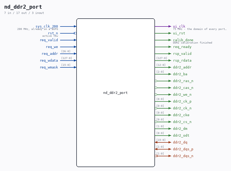
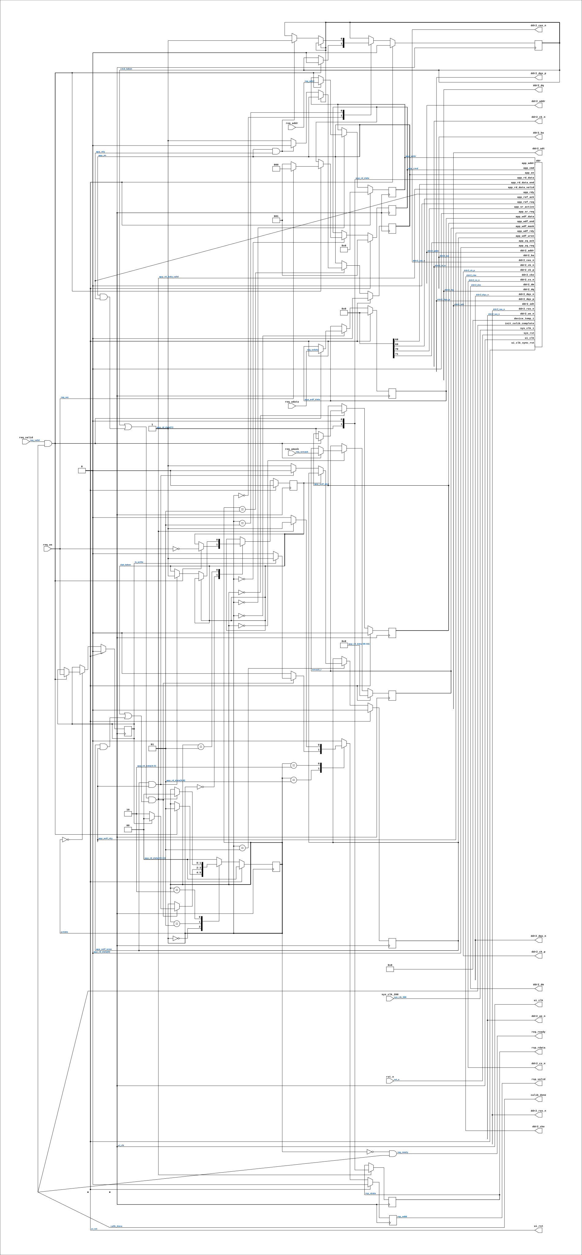
Schematic
Drawn from the Verilog: the yosys netlist of the Nexys 4 DDR build, instance u_ddr2. Sub-modules are boxes (click the picture to open it full size; there every sub-module box links to its page, and every wire shows its Verilog name).
Description
nd_ddr2_port - reusable access port to the Nexys 4 DDR's 128 MiB DDR2 One place that owns the MIG controller and hides its two-handshake command interface behind a plain request/response port. Everything that needs DDR2 on this board uses THIS module: - the memory test in the SD-FAT tool (sd-fat-test/nd_memtest_ddr2.v) - the ND-120 sheet-49 main-memory backend, when that is built (see ../EXTENSIONS-PLAN.md - the backend needs a latency answer first, which the memory test measures and reports) Why a wrapper at all: MIG's native interface has TWO independent handshakes that can complete in either order - the command is taken when app_en & app_rdy, the write data when app_wdf_wren & app_wdf_rdy - and a request must be held until its own handshake fires, then dropped in the SAME cycle it is taken or the command is issued twice. That is easy to get wrong once and impossible to get wrong twice if it lives here. PORT CONTRACT (everything below is in the ui_clk domain) req_valid hold high until req_ready is high in the same cycle req_we 1 = write, 0 = read req_addr address in 16-BIT UNITS and a MULTIPLE OF 8: one transfer moves 128 bits = 8 units. Valid range 0 .. 2^26-1 (the device is 64M x 16 = 128 MiB; app_addr's top bit is unused) req_wdata 128 bits; req_wmask is MIG's active-low byte mask (0 = write that byte), so a partial-word update needs no read-modify- write rsp_valid one cycle: read data is on rsp_rdata, or a write is done One operation is outstanding at a time - simple, and far faster than any ND-120 access rate. Pipelining is a later optimisation, not a change of contract. The MIG core itself is generated by ../ddr2-test/gen_mig.tcl from Digilent's own project file; its port list is read out of the generated ip/ddr/ddr_stub.v, never assumed. Clocking: sys_clk_200 must be 200 MHz and ALREADY BUFFERED - the MIG project sets SystemClock = "No Buffer", so no IBUF/BUFG is inserted for it inside the core. ui_clk comes back out at 75 MHz (600 Mbps, 4:1 PHY). Last reviewed: 20-AUG-2026 Ronny Hansen
Ports
| Direction | Width | Name | Description |
|---|---|---|---|
| input | 1 |
sys_clk_200 |
200 MHz, already on a BUFG |
| input | 1 |
rst_n (active low) |
active low |
| output | 1 |
ui_clk |
75 MHz - the domain of every port signal below |
| output | 1 |
ui_rst |
|
| output | 1 |
calib_done |
DDR2 calibration finished |
| input | 1 |
req_valid |
|
| input | 1 |
req_we |
|
| input | [26:0] |
req_addr |
|
| input | [127:0] |
req_wdata |
|
| input | [15:0] |
req_wmask |
|
| output | 1 |
req_ready |
|
| output | 1 |
rsp_valid |
|
| output | [127:0] |
rsp_rdata |
|
| inout | [15:0] |
ddr2_dq |
|
| inout | [1:0] |
ddr2_dqs_p |
|
| inout | [1:0] |
ddr2_dqs_n (active low) |
|
| output | [12:0] |
ddr2_addr |
|
| output | [2:0] |
ddr2_ba |
|
| output | 1 |
ddr2_ras_n (active low) |
|
| output | 1 |
ddr2_cas_n (active low) |
|
| output | 1 |
ddr2_we_n (active low) |
|
| output | [0:0] |
ddr2_ck_p |
|
| output | [0:0] |
ddr2_ck_n (active low) |
|
| output | [0:0] |
ddr2_cke |
|
| output | [0:0] |
ddr2_cs_n (active low) |
|
| output | [1:0] |
ddr2_dm |
|
| output | [0:0] |
ddr2_odt |
Verilog source
Verilog/fpga/nexys4ddr/ddr2/nd_ddr2_port.v on GitHub.
Show the Verilog of nd_ddr2_port (238 lines)
/****************************************************************************
** nd_ddr2_port - reusable access port to the Nexys 4 DDR's 128 MiB DDR2    **
**                                                                         **
** One place that owns the MIG controller and hides its two-handshake       **
** command interface behind a plain request/response port. Everything that  **
** needs DDR2 on this board uses THIS module:                               **
**                                                                         **
**   - the memory test in the SD-FAT tool (sd-fat-test/nd_memtest_ddr2.v)   **
**   - the ND-120 sheet-49 main-memory backend, when that is built          **
**     (see ../EXTENSIONS-PLAN.md - the backend needs a latency answer      **
**     first, which the memory test measures and reports)                   **
**                                                                         **
** Why a wrapper at all: MIG's native interface has TWO independent         **
** handshakes that can complete in either order - the command is taken when **
** app_en & app_rdy, the write data when app_wdf_wren & app_wdf_rdy - and a **
** request must be held until its own handshake fires, then dropped in the  **
** SAME cycle it is taken or the command is issued twice. That is easy to   **
** get wrong once and impossible to get wrong twice if it lives here.       **
**                                                                         **
** PORT CONTRACT (everything below is in the ui_clk domain)                 **
**   req_valid  hold high until req_ready is high in the same cycle         **
**   req_we     1 = write, 0 = read                                        **
**   req_addr   address in 16-BIT UNITS and a MULTIPLE OF 8: one transfer   **
**              moves 128 bits = 8 units. Valid range 0 .. 2^26-1 (the      **
**              device is 64M x 16 = 128 MiB; app_addr's top bit is unused) **
**   req_wdata  128 bits; req_wmask is MIG's active-low byte mask (0 = write **
**              that byte), so a partial-word update needs no read-modify-  **
**              write                                                       **
**   rsp_valid  one cycle: read data is on rsp_rdata, or a write is done    **
**                                                                         **
** One operation is outstanding at a time - simple, and far faster than any **
** ND-120 access rate. Pipelining is a later optimisation, not a change of  **
** contract.                                                                **
**                                                                         **
** The MIG core itself is generated by ../ddr2-test/gen_mig.tcl from        **
** Digilent's own project file; its port list is read out of the generated  **
** ip/ddr/ddr_stub.v, never assumed.                                        **
**                                                                         **
** Clocking: sys_clk_200 must be 200 MHz and ALREADY BUFFERED - the MIG     **
** project sets SystemClock = "No Buffer", so no IBUF/BUFG is inserted for  **
** it inside the core. ui_clk comes back out at 75 MHz (600 Mbps, 4:1 PHY). **
**                                                                         **
** Last reviewed: 20-AUG-2026                                              **
** Ronny Hansen                                                            **
*****************************************************************************/
`default_nettype none

module nd_ddr2_port (
    input wire sys_clk_200,  // 200 MHz, already on a BUFG
    input wire rst_n,        // active low

    output wire ui_clk,      // 75 MHz - the domain of every port signal below
    output wire ui_rst,
    output wire calib_done,  // DDR2 calibration finished

    input  wire          req_valid,
    input  wire          req_we,
    input  wire [ 26:0]  req_addr,
    input  wire [127:0]  req_wdata,
    // Byte lane mask, ACTIVE LOW like MIG's own: bit n = 0 writes byte n.
    // All zeros writes the whole 128 bits. Used by the storage region, which
    // updates single 32-bit words and must not disturb their neighbours.
    input  wire [ 15:0]  req_wmask,
    output wire          req_ready,
    output reg           rsp_valid,
    output wire [127:0]  rsp_rdata,

    // DDR2 device pins
    inout  wire [15:0] ddr2_dq,
    inout  wire [ 1:0] ddr2_dqs_p,
    inout  wire [ 1:0] ddr2_dqs_n,
    output wire [12:0] ddr2_addr,
    output wire [ 2:0] ddr2_ba,
    output wire        ddr2_ras_n,
    output wire        ddr2_cas_n,
    output wire        ddr2_we_n,
    output wire [ 0:0] ddr2_ck_p,
    output wire [ 0:0] ddr2_ck_n,
    output wire [ 0:0] ddr2_cke,
    output wire [ 0:0] ddr2_cs_n,
    output wire [ 1:0] ddr2_dm,
    output wire [ 0:0] ddr2_odt
);

  localparam CMD_WRITE = 3'd0;
  localparam CMD_READ  = 3'd1;

  reg  [ 26:0] app_addr;
  reg  [  2:0] app_cmd;
  reg          app_en;
  reg  [127:0] app_wdf_data;
  reg  [ 15:0] wmask_r;
  reg          app_wdf_wren, app_wdf_end;
  wire [127:0] app_rd_data;
  wire         app_rd_data_valid;
  wire         app_rdy, app_wdf_rdy;

  ddr u_mig (
      .ddr2_dq   (ddr2_dq),
      .ddr2_dqs_p(ddr2_dqs_p),
      .ddr2_dqs_n(ddr2_dqs_n),
      .ddr2_addr (ddr2_addr),
      .ddr2_ba   (ddr2_ba),
      .ddr2_ras_n(ddr2_ras_n),
      .ddr2_cas_n(ddr2_cas_n),
      .ddr2_we_n (ddr2_we_n),
      .ddr2_ck_p (ddr2_ck_p),
      .ddr2_ck_n (ddr2_ck_n),
      .ddr2_cke  (ddr2_cke),
      .ddr2_cs_n (ddr2_cs_n),
      .ddr2_dm   (ddr2_dm),
      .ddr2_odt  (ddr2_odt),

      .sys_clk_i(sys_clk_200),
      .sys_rst  (rst_n),          // ACTIVE LOW per the MIG project file

      .app_addr         (app_addr),
      .app_cmd          (app_cmd),
      .app_en           (app_en),
      .app_wdf_data     (app_wdf_data),
      .app_wdf_end      (app_wdf_end),
      .app_wdf_mask     (wmask_r),
      .app_wdf_wren     (app_wdf_wren),
      .app_rd_data      (app_rd_data),
      .app_rd_data_end  (),
      .app_rd_data_valid(app_rd_data_valid),
      .app_rdy          (app_rdy),
      .app_wdf_rdy      (app_wdf_rdy),

      .app_sr_req   (1'b0),
      .app_ref_req  (1'b0),
      .app_zq_req   (1'b0),
      .app_sr_active(),
      .app_ref_ack  (),
      .app_zq_ack   (),

      .ui_clk             (ui_clk),
      .ui_clk_sync_rst    (ui_rst),
      .init_calib_complete(calib_done),
      .device_temp_i      (12'd0)
  );

  // rsp_valid is registered, so it lands one cycle AFTER app_rd_data_valid.
  // The controller does not hold app_rd_data that long - capture it.
  reg [127:0] rdata_r;
  always @(posedge ui_clk) begin
    if (app_rd_data_valid) rdata_r <= app_rd_data;
  end
  assign rsp_rdata = rdata_r;

  localparam P_IDLE = 2'd0;
  localparam P_CMD  = 2'd1;
  localparam P_READ = 2'd2;

  reg [1:0] pstate;
  reg       cmd_taken, dat_taken, is_write;

  // A new request is accepted only while idle and calibrated
  assign req_ready = (pstate == P_IDLE) && calib_done;

  always @(posedge ui_clk) begin
    if (ui_rst) begin
      pstate       <= P_IDLE;
      app_en       <= 1'b0;
      app_wdf_wren <= 1'b0;
      app_wdf_end  <= 1'b0;
      app_cmd      <= CMD_READ;
      app_addr     <= 27'd0;
      app_wdf_data <= 128'd0;
      wmask_r      <= 16'h0000;
      cmd_taken    <= 1'b0;
      dat_taken    <= 1'b0;
      is_write     <= 1'b0;
      rsp_valid    <= 1'b0;
    end else begin
      rsp_valid <= 1'b0;

      case (pstate)
        P_IDLE:
        if (req_valid && calib_done) begin
          app_addr     <= req_addr;
          app_cmd      <= req_we ? CMD_WRITE : CMD_READ;
          app_wdf_data <= req_wdata;
          wmask_r      <= req_wmask;
          app_wdf_end  <= 1'b1;
          is_write     <= req_we;
          cmd_taken    <= 1'b0;
          // a read has no write-data phase, so that half is already done
          dat_taken    <= ~req_we;
          pstate       <= P_CMD;
        end

        // Hold each request until its own handshake fires. The later
        // non-blocking write in this block wins, so a request drops in
        // exactly the cycle it is taken - never one cycle later, which
        // would issue the same command twice.
        P_CMD: begin
          if (!cmd_taken) begin
            app_en <= 1'b1;
            if (app_en && app_rdy) begin
              app_en    <= 1'b0;
              cmd_taken <= 1'b1;
            end
          end

          if (!dat_taken) begin
            app_wdf_wren <= 1'b1;
            if (app_wdf_wren && app_wdf_rdy) begin
              app_wdf_wren <= 1'b0;
              dat_taken    <= 1'b1;
            end
          end

          if ((cmd_taken || (app_en && app_rdy)) &&
              (dat_taken || (app_wdf_wren && app_wdf_rdy))) begin
            if (is_write) begin
              rsp_valid <= 1'b1;   // write accepted by the controller
              pstate    <= P_IDLE;
            end else begin
              pstate <= P_READ;
            end
          end
        end

        P_READ:
        if (app_rd_data_valid) begin
          rsp_valid <= 1'b1;
          pstate    <= P_IDLE;
        end

        default: pstate <= P_IDLE;
      endcase
    end
  end

endmodule

`default_nettype wire