nexys4ddr_sd_fat_top
Source: Verilog/fpga/nexys4ddr/sd-fat-test/nexys4ddr_sd_fat_top.v
Hierarchy: not instantiated by any of the 9 build tops (elaborated by yosys).
Module hierarchy - All modules
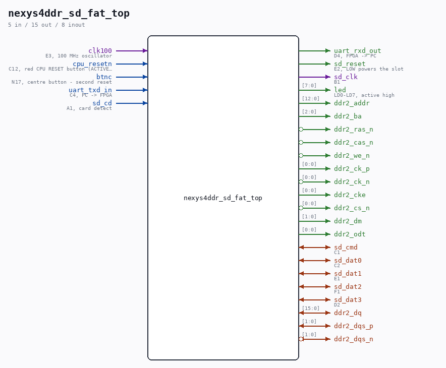
Schematic
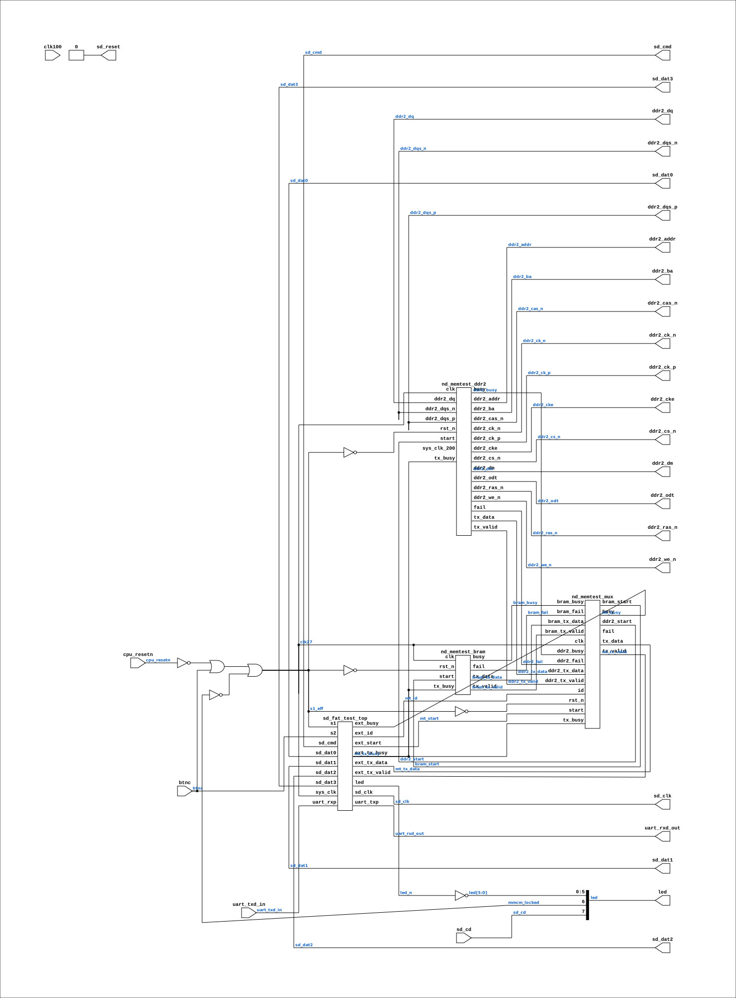
Drawn from the Verilog: no build top uses this module, so it was elaborated from its own file with no defines and default parameters. Sub-modules are boxes (click the picture to open it full size; there every sub-module box links to its page, and every wire shows its Verilog name).
Description
Nexys 4 DDR wrapper for the SD-FAT test (sd_fat_test_top) The test design itself is board-independent (single clock domain, all SD/UART speeds derived from CLK_FREQ by enable dividers) and is reused unchanged from the Tang Nano 20K build, exactly as the Basys3 wrapper does. This wrapper provides: - 27.027 MHz from the 100 MHz oscillator (MMCM x10 / 37), the same CLK_FREQ the Tang hardware-proven build uses, so every divider, watchdog and baud constant stays at its validated value - reset: CPU RESET (active low) or BTNC, plus MMCM lock - LED polarity: the test drives active LOW, the board is active HIGH - UART to the FT2232 at 9600 8N1 THE BOARD DIFFERENCE THAT MATTERS: the microSD slot is ON THE BOARD, not on a Pmod, and its power is gated. Reference manual section 12: after configuration the on-board microcontroller releases the SD bus and "the SD_RESET signal needs to be actively driven low by the FPGA to power the microSD card slot". Without that the slot is dead and every command times out. sd_reset is therefore driven low here. Pins (../Nexys-4-DDR-Master.xdc): SD_SCK B1, SD_CMD C1, SD_DAT C2/E1/F1/D2, SD_CD A1, SD_RESET E2. Build: vivado -mode batch -source build.tcl (see README.md) Last reviewed: 20-AUG-2026 Ronny Hansen
Ports
| Direction | Width | Name | Description |
|---|---|---|---|
| input | 1 |
clk100 |
E3, 100 MHz oscillator |
| input | 1 |
cpu_resetn |
C12, red CPU RESET button (ACTIVE LOW) |
| input | 1 |
btnc |
N17, centre button - second reset |
| input | 1 |
uart_txd_in |
C4, PC -> FPGA |
| output | 1 |
uart_rxd_out |
D4, FPGA -> PC |
| output | 1 |
sd_reset |
E2, LOW powers the slot |
| input | 1 |
sd_cd |
A1, card detect |
| output | 1 |
sd_clk |
B1 |
| inout | 1 |
sd_cmd |
C1 |
| inout | 1 |
sd_dat0 |
C2 |
| inout | 1 |
sd_dat1 |
E1 |
| inout | 1 |
sd_dat2 |
F1 |
| inout | 1 |
sd_dat3 |
D2 |
| output | [7:0] |
led |
LD0-LD7, active high |
| inout | [15:0] |
ddr2_dq |
|
| inout | [1:0] |
ddr2_dqs_p |
|
| inout | [1:0] |
ddr2_dqs_n (active low) |
|
| output | [12:0] |
ddr2_addr |
|
| output | [2:0] |
ddr2_ba |
|
| output | 1 |
ddr2_ras_n (active low) |
|
| output | 1 |
ddr2_cas_n (active low) |
|
| output | 1 |
ddr2_we_n (active low) |
|
| output | [0:0] |
ddr2_ck_p |
|
| output | [0:0] |
ddr2_ck_n (active low) |
|
| output | [0:0] |
ddr2_cke |
|
| output | [0:0] |
ddr2_cs_n (active low) |
|
| output | [1:0] |
ddr2_dm |
|
| output | [0:0] |
ddr2_odt |
Verilog source
Verilog/fpga/nexys4ddr/sd-fat-test/nexys4ddr_sd_fat_top.v on GitHub.
Show the Verilog of nexys4ddr_sd_fat_top (218 lines)
/****************************************************************************
** Nexys 4 DDR wrapper for the SD-FAT test (sd_fat_test_top)               **
**                                                                         **
** The test design itself is board-independent (single clock domain, all   **
** SD/UART speeds derived from CLK_FREQ by enable dividers) and is reused  **
** unchanged from the Tang Nano 20K build, exactly as the Basys3 wrapper   **
** does. This wrapper provides:                                            **
**                                                                         **
**   - 27.027 MHz from the 100 MHz oscillator (MMCM x10 / 37), the same    **
**     CLK_FREQ the Tang hardware-proven build uses, so every divider,     **
**     watchdog and baud constant stays at its validated value             **
**   - reset: CPU RESET (active low) or BTNC, plus MMCM lock               **
**   - LED polarity: the test drives active LOW, the board is active HIGH  **
**   - UART to the FT2232 at 9600 8N1                                      **
**                                                                         **
** THE BOARD DIFFERENCE THAT MATTERS: the microSD slot is ON THE BOARD,    **
** not on a Pmod, and its power is gated. Reference manual section 12:     **
** after configuration the on-board microcontroller releases the SD bus    **
** and "the SD_RESET signal needs to be actively driven low by the FPGA    **
** to power the microSD card slot". Without that the slot is dead and      **
** every command times out. sd_reset is therefore driven low here.         **
**                                                                         **
** Pins (../Nexys-4-DDR-Master.xdc): SD_SCK B1, SD_CMD C1,                 **
** SD_DAT C2/E1/F1/D2, SD_CD A1, SD_RESET E2.                              **
**                                                                         **
** Build: vivado -mode batch -source build.tcl   (see README.md)           **
**                                                                         **
** Last reviewed: 20-AUG-2026                                              **
** Ronny Hansen                                                            **
*****************************************************************************/

module nexys4ddr_sd_fat_top (
    input clk100,      // E3, 100 MHz oscillator
    input cpu_resetn,  // C12, red CPU RESET button (ACTIVE LOW)
    input btnc,        // N17, centre button - second reset

    input  uart_txd_in,   // C4, PC -> FPGA
    output uart_rxd_out,  // D4, FPGA -> PC

    // On-board microSD slot
    output sd_reset,  // E2, LOW powers the slot
    input  sd_cd,     // A1, card detect
    output sd_clk,    // B1
    inout  sd_cmd,    // C1
    inout  sd_dat0,   // C2
    inout  sd_dat1,   // E1
    inout  sd_dat2,   // F1
    inout  sd_dat3,   // D2

    output [7:0] led,  // LD0-LD7, active high

    // DDR2 - 128 MiB Micron MT47H64M16HR. Pin constraints come from the MIG
    // core's own generated XDC, which matches on THESE port names.
    inout  [15:0] ddr2_dq,
    inout  [ 1:0] ddr2_dqs_p,
    inout  [ 1:0] ddr2_dqs_n,
    output [12:0] ddr2_addr,
    output [ 2:0] ddr2_ba,
    output        ddr2_ras_n,
    output        ddr2_cas_n,
    output        ddr2_we_n,
    output [ 0:0] ddr2_ck_p,
    output [ 0:0] ddr2_ck_n,
    output [ 0:0] ddr2_cke,
    output [ 0:0] ddr2_cs_n,
    output [ 1:0] ddr2_dm,
    output [ 0:0] ddr2_odt
);

  /**********************************************
  *  27.027 MHz from 100 MHz (VCO 1000 / 37)    *
  ***********************************************/
  wire clk27_pre, clk200_pre, clkfb_out, clkfb_in, mmcm_locked;
  wire clk27, clk200;

  MMCME2_BASE #(
      .BANDWIDTH       ("OPTIMIZED"),
      .CLKFBOUT_MULT_F (10.0),  // VCO = 100 * 10 = 1000 MHz
      .CLKIN1_PERIOD   (10.0),  // 100 MHz input
      .CLKOUT0_DIVIDE_F(37.0),  // 1000 / 37 = 27.027 MHz - console + SD
      .CLKOUT1_DIVIDE  (5),     // 1000 / 5  = 200 MHz    - DDR2 controller
      .DIVCLK_DIVIDE   (1),
      .STARTUP_WAIT    ("FALSE")
  ) mmcm_sd_clk (
      .CLKIN1  (clk100),
      .CLKFBIN (clkfb_in),
      .CLKFBOUT(clkfb_out),
      .CLKOUT0 (clk27_pre),
      .CLKOUT1 (clk200_pre),
      .LOCKED  (mmcm_locked),
      .PWRDWN  (1'b0),
      .RST     (1'b0)
  );
  BUFG bufg_fb  (.I(clkfb_out), .O(clkfb_in));
  BUFG bufg_27  (.I(clk27_pre), .O(clk27));
  // The MIG project says SystemClock = "No Buffer", so the 200 MHz must
  // arrive already buffered - MIG does not insert a BUFG of its own.
  BUFG bufg_200 (.I(clk200_pre), .O(clk200));

  // Power the card slot. This must be low for anything below to work.
  assign sd_reset = 1'b0;

  // Full reset while either button is pressed or the MMCM is unlocked
  wire s1_eff = ~cpu_resetn | btnc | ~mmcm_locked;

  wire [5:0] led_n;  // active low from the test design
  assign led[5:0] = ~led_n;
  assign led[6]   = mmcm_locked;
  assign led[7]   = sd_cd;  // raw card-detect line (polarity not documented)

  /**********************************************
  *  Memory tests, reachable from the SD menu   *
  *  (SDFAT_EXT_TEST): key B = ND-120 memory    *
  *  path, key M = DDR2. They print through the *
  *  test design's own UART.                    *
  ***********************************************/
  wire       mt_start;
  wire [3:0] mt_id;
  wire       mt_busy;
  wire [7:0] mt_tx_data;
  wire       mt_tx_valid;
  wire       mt_fail;
  wire       mt_tx_busy;

  wire       bram_start, bram_busy, bram_tx_valid, bram_fail;
  wire [7:0] bram_tx_data;
  wire       ddr2_start, ddr2_busy, ddr2_tx_valid, ddr2_fail;
  wire [7:0] ddr2_tx_data;

  nd_memtest_mux u_mt (
      .clk(clk27),
      .rst_n(~s1_eff),
      .start(mt_start),
      .id(mt_id),
      .busy(mt_busy),
      .tx_data(mt_tx_data),
      .tx_valid(mt_tx_valid),
      .tx_busy(mt_tx_busy),
      .fail(mt_fail),

      .bram_start(bram_start),
      .bram_busy(bram_busy),
      .bram_tx_data(bram_tx_data),
      .bram_tx_valid(bram_tx_valid),
      .bram_fail(bram_fail),

      .ddr2_start(ddr2_start),
      .ddr2_busy(ddr2_busy),
      .ddr2_tx_data(ddr2_tx_data),
      .ddr2_tx_valid(ddr2_tx_valid),
      .ddr2_fail(ddr2_fail)
  );

  nd_memtest_ddr2 u_ddr2_test (
      .clk        (clk27),
      .rst_n      (~s1_eff),
      .start      (ddr2_start),
      .busy       (ddr2_busy),
      .tx_data    (ddr2_tx_data),
      .tx_valid   (ddr2_tx_valid),
      .tx_busy    (mt_tx_busy),
      .fail       (ddr2_fail),
      .sys_clk_200(clk200),

      .ddr2_dq   (ddr2_dq),
      .ddr2_dqs_p(ddr2_dqs_p),
      .ddr2_dqs_n(ddr2_dqs_n),
      .ddr2_addr (ddr2_addr),
      .ddr2_ba   (ddr2_ba),
      .ddr2_ras_n(ddr2_ras_n),
      .ddr2_cas_n(ddr2_cas_n),
      .ddr2_we_n (ddr2_we_n),
      .ddr2_ck_p (ddr2_ck_p),
      .ddr2_ck_n (ddr2_ck_n),
      .ddr2_cke  (ddr2_cke),
      .ddr2_cs_n (ddr2_cs_n),
      .ddr2_dm   (ddr2_dm),
      .ddr2_odt  (ddr2_odt)
  );

  nd_memtest_bram u_bram_test (
      .clk(clk27),
      .rst_n(~s1_eff),
      .start(bram_start),
      .busy(bram_busy),
      .tx_data(bram_tx_data),
      .tx_valid(bram_tx_valid),
      .tx_busy(mt_tx_busy),
      .fail(bram_fail)
  );

  sd_fat_test_top #(
      .CLK_FREQ(27_027_027)  // exact MMCM output; all dividers derive from it
  ) u_test (
      .sys_clk (clk27),
      .s1      (s1_eff),
      .s2      (btnc),
      .uart_rxp(uart_txd_in),
      .uart_txp(uart_rxd_out),

      .sd_clk (sd_clk),
      .sd_cmd (sd_cmd),
      .sd_dat0(sd_dat0),
      .sd_dat1(sd_dat1),
      .sd_dat2(sd_dat2),
      .sd_dat3(sd_dat3),

      .led(led_n),

      .ext_start(mt_start),
      .ext_id(mt_id),
      .ext_busy(mt_busy),
      .ext_tx_data(mt_tx_data),
      .ext_tx_valid(mt_tx_valid),
      .ext_tx_busy(mt_tx_busy)
  );

endmodule