nd_memtest_ddr2
Source: Verilog/fpga/nexys4ddr/sd-fat-test/nd_memtest_ddr2.v
Hierarchy: not instantiated by any of the 9 build tops (elaborated by yosys).
Module hierarchy - All modules
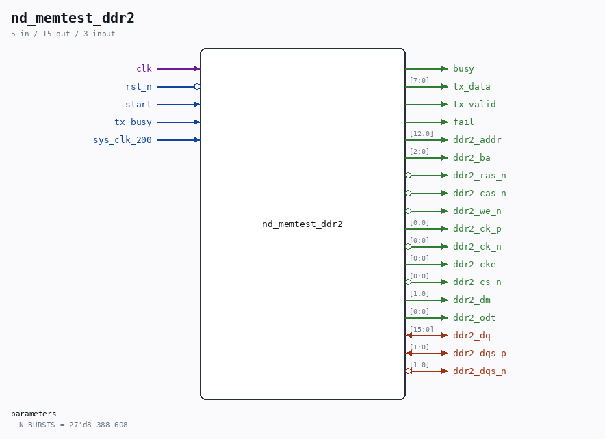
Schematic
Drawn from the Verilog: no build top uses this module, so it was elaborated from its own file with no defines and default parameters. Sub-modules are boxes (click the picture to open it full size; there every sub-module box links to its page, and every wire shows its Verilog name).

Description
DDR2 memory test for the Nexys 4 DDR, as a character stream Runs as menu command M in the SD-FAT tool. Two jobs: 1. VALIDATE the memory. Writes an address-derived pattern over the whole 128 MiB, reads it back and verifies every word. 2. MEASURE WORST-CASE READ LATENCY, in ui_clk cycles, from the cycle a read is accepted to the cycle its data comes back. This is not a nice-to-have: it is the number that decides how ND-120 main memory can be built on this board at all. The ND-120's sheet-49 memory protocol has a FIXED deadline and no wait states - measured over 25,008 accesses, the column address is known at cycle N+1 and read data must be valid by the start of N+4 (Verilog/docs/nd120-dram-memory.md). That is three CPU cycles: 180 ns at 16.667 MHz, 90 ns at 33.333 MHz. One ui_clk cycle is 13.33 ns, so the budget is about 13 ui_clk cycles at the slow CPU clock. If the measured worst case fits, a direct sheet-49 backend is possible; if it does not - and a DDR2 refresh alone is tRFC = 127.5 ns - then the backend needs a cache in front, or the CPU clock must be stalled on a miss. See ../EXTENSIONS-PLAN.md section "Stage 2". The controller itself lives in ../ddr2/nd_ddr2_port.v, shared with the future ND-120 memory backend - this test exercises the SAME access path the CPU will use, which is the point of testing it here. CLOCK DOMAINS: the test runs in ui_clk (75 MHz), the console at 27.027 MHz. start, busy, fail and every character cross with two-flop synchronisers and a request/acknowledge toggle; the data byte is held stable until the far side takes it. build.tcl declares the two clocks asynchronous - without that Vivado times the crossings as related clocks and demands 0.333 ns, which nothing can meet (measured: -3.304 ns). Report: DDR2 CALIB OK DDR2 WRITE 00 ... (one line per 16 MiB) DDR2 READ 00 ... DDR2 RDLAT MAX 000n CYC DDR2 PASS (or DDR2 FAIL AT xxxxxxx then DDR2 ERRS nnnn) Last reviewed: 20-AUG-2026 Ronny Hansen
Parameters
| Parameter | Default |
|---|---|
N_BURSTS |
27'd8_388_608 |
Ports
| Direction | Width | Name | Description |
|---|---|---|---|
| input | 1 |
clk |
|
| input | 1 |
rst_n (active low) |
|
| input | 1 |
start |
|
| output | 1 |
busy |
|
| output | [7:0] |
tx_data |
|
| output | 1 |
tx_valid |
|
| input | 1 |
tx_busy |
|
| output | 1 |
fail |
|
| input | 1 |
sys_clk_200 |
|
| inout | [15:0] |
ddr2_dq |
|
| inout | [1:0] |
ddr2_dqs_p |
|
| inout | [1:0] |
ddr2_dqs_n (active low) |
|
| output | [12:0] |
ddr2_addr |
|
| output | [2:0] |
ddr2_ba |
|
| output | 1 |
ddr2_ras_n (active low) |
|
| output | 1 |
ddr2_cas_n (active low) |
|
| output | 1 |
ddr2_we_n (active low) |
|
| output | [0:0] |
ddr2_ck_p |
|
| output | [0:0] |
ddr2_ck_n (active low) |
|
| output | [0:0] |
ddr2_cke |
|
| output | [0:0] |
ddr2_cs_n (active low) |
|
| output | [1:0] |
ddr2_dm |
|
| output | [0:0] |
ddr2_odt |
Verilog source
Verilog/fpga/nexys4ddr/sd-fat-test/nd_memtest_ddr2.v on GitHub.
Show the Verilog of nd_memtest_ddr2 (581 lines)
/****************************************************************************
** DDR2 memory test for the Nexys 4 DDR, as a character stream **
** **
** Runs as menu command M in the SD-FAT tool. Two jobs: **
** **
** 1. VALIDATE the memory. Writes an address-derived pattern over the **
** whole 128 MiB, reads it back and verifies every word. **
** **
** 2. MEASURE WORST-CASE READ LATENCY, in ui_clk cycles, from the cycle a **
** read is accepted to the cycle its data comes back. This is not a **
** nice-to-have: it is the number that decides how ND-120 main memory **
** can be built on this board at all. **
** **
** The ND-120's sheet-49 memory protocol has a FIXED deadline and no **
** wait states - measured over 25,008 accesses, the column address is **
** known at cycle N+1 and read data must be valid by the start of N+4 **
** (Verilog/docs/nd120-dram-memory.md). That is three CPU cycles: 180 ns**
** at 16.667 MHz, 90 ns at 33.333 MHz. One ui_clk cycle is 13.33 ns, so **
** the budget is about 13 ui_clk cycles at the slow CPU clock. If the **
** measured worst case fits, a direct sheet-49 backend is possible; if **
** it does not - and a DDR2 refresh alone is tRFC = 127.5 ns - then the **
** backend needs a cache in front, or the CPU clock must be stalled on **
** a miss. See ../EXTENSIONS-PLAN.md section "Stage 2". **
** **
** The controller itself lives in ../ddr2/nd_ddr2_port.v, shared with the **
** future ND-120 memory backend - this test exercises the SAME access path **
** the CPU will use, which is the point of testing it here. **
** **
** CLOCK DOMAINS: the test runs in ui_clk (75 MHz), the console at **
** 27.027 MHz. start, busy, fail and every character cross with two-flop **
** synchronisers and a request/acknowledge toggle; the data byte is held **
** stable until the far side takes it. build.tcl declares the two clocks **
** asynchronous - without that Vivado times the crossings as related clocks **
** and demands 0.333 ns, which nothing can meet (measured: -3.304 ns). **
** **
** Report: **
** DDR2 CALIB OK **
** DDR2 WRITE 00 ... (one line per 16 MiB) **
** DDR2 READ 00 ... **
** DDR2 RDLAT MAX 000n CYC **
** DDR2 PASS (or DDR2 FAIL AT xxxxxxx then DDR2 ERRS nnnn) **
** **
** Last reviewed: 20-AUG-2026 **
** Ronny Hansen **
*****************************************************************************/
`default_nettype none
module nd_memtest_ddr2 #(
// Transfers to cover. The whole device is 2^26 sixteen-bit units and one
// transfer moves 8 of them: 2^26 / 8 = 8,388,608.
parameter [26:0] N_BURSTS = 27'd8_388_608
) (
// console domain (27.027 MHz)
input wire clk,
input wire rst_n,
input wire start,
output wire busy,
output wire [7:0] tx_data,
output wire tx_valid,
input wire tx_busy,
output wire fail,
// 200 MHz for the controller, already on a BUFG
input wire sys_clk_200,
// DDR2 pins
inout wire [15:0] ddr2_dq,
inout wire [ 1:0] ddr2_dqs_p,
inout wire [ 1:0] ddr2_dqs_n,
output wire [12:0] ddr2_addr,
output wire [ 2:0] ddr2_ba,
output wire ddr2_ras_n,
output wire ddr2_cas_n,
output wire ddr2_we_n,
output wire [ 0:0] ddr2_ck_p,
output wire [ 0:0] ddr2_ck_n,
output wire [ 0:0] ddr2_cke,
output wire [ 0:0] ddr2_cs_n,
output wire [ 1:0] ddr2_dm,
output wire [ 0:0] ddr2_odt
);
/*******************************************************************
* The shared DDR2 access port - the same one the ND-120 memory
* backend will use
*******************************************************************/
wire ui_clk, ui_rst, calib_done;
reg req_valid, req_we;
reg [ 26:0] req_addr;
reg [127:0] req_wdata;
reg [ 15:0] req_wmask;
wire req_ready, rsp_valid;
wire [127:0] rsp_rdata;
nd_ddr2_port u_port (
.sys_clk_200(sys_clk_200),
.rst_n (rst_n),
.ui_clk (ui_clk),
.ui_rst (ui_rst),
.calib_done (calib_done),
.req_valid(req_valid),
.req_we (req_we),
.req_addr (req_addr),
.req_wdata(req_wdata),
.req_wmask(req_wmask), // whole-beat writes use 0000; the MASKW
// phase drives the region's byte-lane masks
.req_ready(req_ready),
.rsp_valid(rsp_valid),
.rsp_rdata(rsp_rdata),
.ddr2_dq (ddr2_dq),
.ddr2_dqs_p(ddr2_dqs_p),
.ddr2_dqs_n(ddr2_dqs_n),
.ddr2_addr (ddr2_addr),
.ddr2_ba (ddr2_ba),
.ddr2_ras_n(ddr2_ras_n),
.ddr2_cas_n(ddr2_cas_n),
.ddr2_we_n (ddr2_we_n),
.ddr2_ck_p (ddr2_ck_p),
.ddr2_ck_n (ddr2_ck_n),
.ddr2_cke (ddr2_cke),
.ddr2_cs_n (ddr2_cs_n),
.ddr2_dm (ddr2_dm),
.ddr2_odt (ddr2_odt)
);
/*******************************************************************
* start / busy / fail across the clock domains
*******************************************************************/
reg start_tgl;
always @(posedge clk) begin
if (!rst_n) start_tgl <= 1'b0;
else if (start) start_tgl <= ~start_tgl;
end
reg s1, s2, s3;
always @(posedge ui_clk) begin
if (ui_rst) begin s1 <= 1'b0; s2 <= 1'b0; s3 <= 1'b0; end
else begin s1 <= start_tgl; s2 <= s1; s3 <= s2; end
end
wire ui_start = s2 ^ s3;
reg ui_busy, ui_fail;
reg b1, b2, f1, f2;
always @(posedge clk) begin
if (!rst_n) begin b1 <= 1'b0; b2 <= 1'b0; f1 <= 1'b0; f2 <= 1'b0; end
else begin b1 <= ui_busy; b2 <= b1; f1 <= ui_fail; f2 <= f1; end
end
assign busy = b2;
assign fail = f2;
/*******************************************************************
* Character channel, ui_clk -> console, request/acknowledge toggle
*******************************************************************/
reg [7:0] ch_data;
reg ch_req;
reg r1, r2;
reg ack_tgl;
always @(posedge clk) begin
if (!rst_n) begin r1 <= 1'b0; r2 <= 1'b0; end
else begin r1 <= ch_req; r2 <= r1; end
end
wire pending = (r2 ^ ack_tgl);
reg [7:0] tx_data_r;
reg tx_valid_r;
always @(posedge clk) begin
if (!rst_n) begin
tx_valid_r <= 1'b0;
tx_data_r <= 8'd0;
ack_tgl <= 1'b0;
end else begin
tx_valid_r <= 1'b0;
if (pending && !tx_busy && !tx_valid_r) begin
tx_data_r <= ch_data; // held by the ui side until acknowledged
tx_valid_r <= 1'b1;
ack_tgl <= r2;
end
end
end
assign tx_data = tx_data_r;
assign tx_valid = tx_valid_r;
reg a1, a2;
always @(posedge ui_clk) begin
if (ui_rst) begin a1 <= 1'b0; a2 <= 1'b0; end
else begin a1 <= ack_tgl; a2 <= a1; end
end
wire ch_ready = (a2 == ch_req);
/*******************************************************************
* Line assembler (ui_clk)
*******************************************************************/
reg [7:0] line[0:31];
reg [5:0] line_len, line_ptr;
function [7:0] hexch;
input [3:0] v;
begin
hexch = (v < 4'd10) ? (8'h30 + {4'b0, v}) : (8'h41 + {4'b0, (v - 4'd10)});
end
endfunction
/*******************************************************************
* Test FSM (ui_clk)
*
* Pattern: transfer n holds eight 16-bit words, word i = n + i. Every
* lane is distinct, so a stuck address bit returns a neighbour's data
* rather than something that happens to match.
*******************************************************************/
localparam S_IDLE = 5'd0;
localparam S_CALIB = 5'd1;
localparam S_WR = 5'd2;
localparam S_WR_WAIT = 5'd3;
localparam S_RD = 5'd4;
localparam S_RD_WAIT = 5'd5;
localparam S_NEXT = 5'd6;
localparam S_PROG = 5'd7;
localparam S_EMIT = 5'd8;
localparam S_LATLINE = 5'd9;
localparam S_RESULT = 5'd10;
localparam S_ERRLINE = 5'd11;
localparam S_END = 5'd12;
// MASKW: byte-masked partial writes - the storage region's idiom
// (nd_ddr2_storage lane_mask), which the full-beat sweep never touches
localparam S_MW = 5'd13; // full-beat base write
localparam S_MW_W = 5'd14;
localparam S_MP = 5'd15; // masked 4-byte write
localparam S_MP_W = 5'd16;
localparam S_MR = 5'd17; // read back, verify lanes
localparam S_MR_W = 5'd18;
localparam S_MWLINE = 5'd19;
reg [ 4:0] state, after_emit;
reg [26:0] burst;
reg [31:0] calib_wd;
reg [15:0] nerr;
reg [26:0] first_bad;
reg have_bad, phase_read;
reg [ 7:0] prog_mib;
// read-latency measurement, in ui_clk cycles
reg [15:0] lat_cnt, lat_max;
// MASKW bookkeeping
reg [ 3:0] mw_i;
reg [ 7:0] mw_err;
reg [127:0] mw_exp;
wire [ 1:0] mw_lane = mw_i[1:0];
wire [26:0] mw_addr = {4'd0, mw_i, 16'h0000, 3'b000};
wire [127:0] mw_base = {32'hDDCC0000 | {28'd0,mw_i}, 32'h99880000 | {28'd0,mw_i},
32'h55440000 | {28'd0,mw_i}, 32'h11000000 | {28'd0,mw_i}};
wire [31:0] mw_bword = 32'hC3C30000 | {28'd0, mw_i};
wire [15:0] mw_mask = ~(16'h000F << {mw_lane, 2'b00});
wire [26:0] addr = {burst[23:0], 3'b000};
wire [127:0] pattern = {
burst[15:0] + 16'd7, burst[15:0] + 16'd6,
burst[15:0] + 16'd5, burst[15:0] + 16'd4,
burst[15:0] + 16'd3, burst[15:0] + 16'd2,
burst[15:0] + 16'd1, burst[15:0] + 16'd0
};
reg [127:0] expect_r;
always @(posedge ui_clk) begin
if (ui_rst) begin
state <= S_IDLE;
ui_busy <= 1'b0;
ui_fail <= 1'b0;
req_valid <= 1'b0;
req_we <= 1'b0;
req_addr <= 27'd0;
req_wdata <= 128'd0;
burst <= 27'd0;
nerr <= 16'd0;
have_bad <= 1'b0;
first_bad <= 27'd0;
ch_req <= 1'b0;
ch_data <= 8'd0;
line_len <= 6'd0;
line_ptr <= 6'd0;
prog_mib <= 8'd0;
phase_read <= 1'b0;
calib_wd <= 32'd0;
lat_cnt <= 16'd0;
lat_max <= 16'd0;
expect_r <= 128'd0;
req_wmask <= 16'h0000;
mw_i <= 4'd0;
mw_err <= 8'd0;
mw_exp <= 128'd0;
end else begin
case (state)
S_IDLE: begin
req_valid <= 1'b0;
ui_busy <= 1'b0;
if (ui_start) begin
ui_busy <= 1'b1;
ui_fail <= 1'b0;
nerr <= 16'd0;
have_bad <= 1'b0;
burst <= 27'd0;
prog_mib <= 8'd0;
phase_read <= 1'b0;
calib_wd <= 32'd0;
lat_max <= 16'd0;
state <= S_CALIB;
end
end
// The controller calibrates itself after reset; this only reports
// whether it finished. 2^26 cycles at 75 MHz is about 0.9 s.
S_CALIB: begin
calib_wd <= calib_wd + 32'd1;
if (calib_done) begin
line[0]<="D"; line[1]<="D"; line[2]<="R"; line[3]<="2"; line[4]<=" ";
line[5]<="C"; line[6]<="A"; line[7]<="L"; line[8]<="I"; line[9]<="B";
line[10]<=" "; line[11]<="O"; line[12]<="K";
line[13]<=8'h0D; line[14]<=8'h0A;
line_len <= 6'd15;
line_ptr <= 6'd0;
after_emit <= S_WR;
state <= S_EMIT;
end else if (calib_wd[26]) begin
line[0]<="D"; line[1]<="D"; line[2]<="R"; line[3]<="2"; line[4]<=" ";
line[5]<="C"; line[6]<="A"; line[7]<="L"; line[8]<="I"; line[9]<="B";
line[10]<=" "; line[11]<="T"; line[12]<="I"; line[13]<="M"; line[14]<="E";
line[15]<="O"; line[16]<="U"; line[17]<="T";
line[18]<=8'h0D; line[19]<=8'h0A;
line_len <= 6'd20;
line_ptr <= 6'd0;
ui_fail <= 1'b1;
after_emit <= S_END;
state <= S_EMIT;
end
end
// ---- write ----------------------------------------------------
S_WR: begin
req_we <= 1'b1;
req_addr <= addr;
req_wdata <= pattern;
req_valid <= 1'b1;
if (req_valid && req_ready) begin
req_valid <= 1'b0; // dropped in the cycle it is accepted
state <= S_WR_WAIT;
end
end
S_WR_WAIT:
if (rsp_valid) state <= S_NEXT;
// ---- read, verify, and time it --------------------------------
S_RD: begin
req_we <= 1'b0;
req_addr <= addr;
expect_r <= pattern;
req_valid <= 1'b1;
if (req_valid && req_ready) begin
req_valid <= 1'b0;
lat_cnt <= 16'd0;
state <= S_RD_WAIT;
end
end
S_RD_WAIT: begin
lat_cnt <= lat_cnt + 16'd1;
if (rsp_valid) begin
if (lat_cnt > lat_max) lat_max <= lat_cnt;
if (rsp_rdata != expect_r) begin
if (nerr != 16'hFFFF) nerr <= nerr + 16'd1;
ui_fail <= 1'b1;
if (!have_bad) begin
have_bad <= 1'b1;
first_bad <= addr;
end
end
state <= S_NEXT;
end
end
S_NEXT:
if (burst == N_BURSTS - 27'd1) begin
if (!phase_read) begin
burst <= 27'd0;
phase_read <= 1'b1;
prog_mib <= 8'd0;
state <= S_PROG;
end else begin
state <= S_LATLINE;
end
end else begin
burst <= burst + 27'd1;
// 16 MiB = 1,048,576 transfers
if (burst[19:0] == 20'hFFFFF) begin
prog_mib <= prog_mib + 8'd1;
state <= S_PROG;
end else begin
state <= phase_read ? S_RD : S_WR;
end
end
S_PROG: begin
line[0]<="D"; line[1]<="D"; line[2]<="R"; line[3]<="2"; line[4]<=" ";
if (!phase_read) begin
line[5]<="W"; line[6]<="R"; line[7]<="I"; line[8]<="T"; line[9]<="E";
line[10]<=" ";
line[11]<=hexch(prog_mib[7:4]);
line[12]<=hexch(prog_mib[3:0]);
line[13]<=8'h0D; line[14]<=8'h0A;
line_len <= 6'd15;
end else begin
line[5]<="R"; line[6]<="E"; line[7]<="A"; line[8]<="D"; line[9]<=" ";
line[10]<=hexch(prog_mib[7:4]);
line[11]<=hexch(prog_mib[3:0]);
line[12]<=8'h0D; line[13]<=8'h0A;
line_len <= 6'd14;
end
line_ptr <= 6'd0;
after_emit <= phase_read ? S_RD : S_WR;
state <= S_EMIT;
end
S_EMIT:
if (line_ptr == line_len) begin
state <= after_emit;
end else if (ch_ready) begin
ch_data <= line[line_ptr[4:0]];
ch_req <= ~ch_req;
line_ptr <= line_ptr + 6'd1;
end
// "DDR2 RDLAT MAX nnnn CYC" - the number that decides whether an
// ND-120 sheet-49 backend can meet the no-wait-state deadline
S_LATLINE: begin
line[0]<="D"; line[1]<="D"; line[2]<="R"; line[3]<="2"; line[4]<=" ";
line[5]<="R"; line[6]<="D"; line[7]<="L"; line[8]<="A"; line[9]<="T";
line[10]<=" "; line[11]<="M"; line[12]<="A"; line[13]<="X"; line[14]<=" ";
line[15]<=hexch(lat_max[15:12]);
line[16]<=hexch(lat_max[11:8]);
line[17]<=hexch(lat_max[7:4]);
line[18]<=hexch(lat_max[3:0]);
line[19]<=" "; line[20]<="C"; line[21]<="Y"; line[22]<="C";
line[23]<=8'h0D; line[24]<=8'h0A;
line_len <= 6'd25;
line_ptr <= 6'd0;
after_emit <= S_MW;
mw_i <= 4'd0;
mw_err <= 8'd0;
state <= S_EMIT;
end
// ---- MASKW: base beat, masked lane update, verify ------------
S_MW: begin
req_we <= 1'b1;
req_addr <= mw_addr;
req_wdata <= mw_base;
req_wmask <= 16'h0000;
req_valid <= 1'b1;
if (req_valid && req_ready) begin
req_valid <= 1'b0;
state <= S_MW_W;
end
end
S_MW_W: if (rsp_valid) state <= S_MP;
S_MP: begin
req_we <= 1'b1;
req_addr <= mw_addr;
req_wdata <= {4{mw_bword}}; // the region's exact write shape
req_wmask <= mw_mask;
req_valid <= 1'b1;
if (req_valid && req_ready) begin
req_valid <= 1'b0;
state <= S_MP_W;
end
end
S_MP_W: if (rsp_valid) state <= S_MR;
S_MR: begin
req_we <= 1'b0;
req_addr <= mw_addr;
req_wmask <= 16'h0000;
case (mw_lane)
2'd0: mw_exp <= {mw_base[127:32], mw_bword};
2'd1: mw_exp <= {mw_base[127:64], mw_bword, mw_base[31:0]};
2'd2: mw_exp <= {mw_base[127:96], mw_bword, mw_base[63:0]};
2'd3: mw_exp <= {mw_bword, mw_base[95:0]};
endcase
req_valid <= 1'b1;
if (req_valid && req_ready) begin
req_valid <= 1'b0;
state <= S_MR_W;
end
end
S_MR_W:
if (rsp_valid) begin
if (rsp_rdata != mw_exp) mw_err <= mw_err + 8'd1;
if (mw_i == 4'd15) state <= S_MWLINE;
else begin
mw_i <= mw_i + 4'd1;
state <= S_MW;
end
end
S_MWLINE: begin
line[0]<="M"; line[1]<="A"; line[2]<="S"; line[3]<="K"; line[4]<="W";
line[5]<=" ";
if (mw_err == 8'd0) begin
line[6]<="P"; line[7]<="A"; line[8]<="S"; line[9]<="S";
line[10]<=8'h0D; line[11]<=8'h0A;
line_len <= 6'd12;
end else begin
line[6]<="F"; line[7]<="A"; line[8]<="I"; line[9]<="L"; line[10]<=" ";
line[11]<=hexch(mw_err[7:4]);
line[12]<=hexch(mw_err[3:0]);
line[13]<=8'h0D; line[14]<=8'h0A;
line_len <= 6'd15;
ui_fail <= 1'b1;
end
line_ptr <= 6'd0;
after_emit <= S_RESULT;
state <= S_EMIT;
end
S_RESULT: begin
line[0]<="D"; line[1]<="D"; line[2]<="R"; line[3]<="2"; line[4]<=" ";
if (!ui_fail) begin
line[5]<="P"; line[6]<="A"; line[7]<="S"; line[8]<="S";
line[9]<=8'h0D; line[10]<=8'h0A;
line_len <= 6'd11;
after_emit <= S_END;
end else begin
line[5]<="F"; line[6]<="A"; line[7]<="I"; line[8]<="L"; line[9]<=" ";
line[10]<="A"; line[11]<="T"; line[12]<=" ";
line[13]<=hexch({1'b0, first_bad[26:24]});
line[14]<=hexch(first_bad[23:20]);
line[15]<=hexch(first_bad[19:16]);
line[16]<=hexch(first_bad[15:12]);
line[17]<=hexch(first_bad[11:8]);
line[18]<=hexch(first_bad[7:4]);
line[19]<=hexch(first_bad[3:0]);
line[20]<=8'h0D; line[21]<=8'h0A;
line_len <= 6'd22;
after_emit <= S_ERRLINE;
end
line_ptr <= 6'd0;
state <= S_EMIT;
end
S_ERRLINE: begin
line[0]<="D"; line[1]<="D"; line[2]<="R"; line[3]<="2"; line[4]<=" ";
line[5]<="E"; line[6]<="R"; line[7]<="R"; line[8]<="S"; line[9]<=" ";
line[10]<=hexch(nerr[15:12]);
line[11]<=hexch(nerr[11:8]);
line[12]<=hexch(nerr[7:4]);
line[13]<=hexch(nerr[3:0]);
line[14]<=8'h0D; line[15]<=8'h0A;
line_len <= 6'd16;
line_ptr <= 6'd0;
after_emit <= S_END;
state <= S_EMIT;
end
S_END: begin
req_valid <= 1'b0;
ui_busy <= 1'b0;
state <= S_IDLE;
end
default: state <= S_IDLE;
endcase
end
end
endmodule
`default_nettype wire