MEM_RAM_49_DDR2
Source: Verilog/fpga/nexys4ddr/ddr2/MEM_RAM_49_DDR2.v
Where it sits (Nexys): nd120_nexys4ddr_top > ND120_CORE > ND3202D > MEM_43 > MEM_RAM_49_DDR2
- instance path: CORE.CPU_BOARD.MEM.RAM
Used in: MEM_43 (Nexys, MEGA65 R3)
Contains: no other modules.
Module hierarchy - All modules
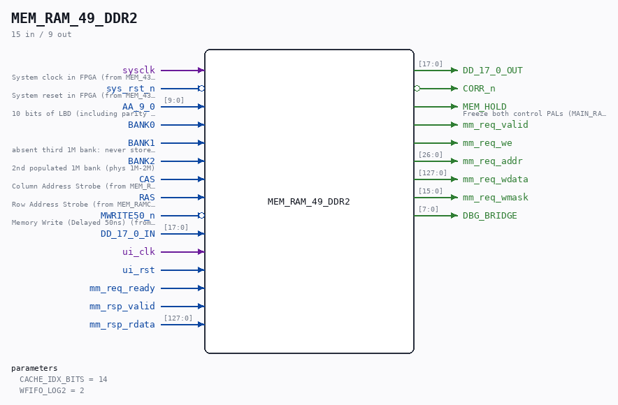
Schematic
Schematic not generated: netlistsvg did not finish in 300 s (16856 cells, 483 wires).
Description
ND120 CPU, MM&M MEM/RAM - DDR2 backend (Nexys 4 DDR) Drop-in replacement for the sheet-49 RAM (MEM_RAM_49) that maps the ND-120 DRAM protocol onto the board's 128 MiB DDR2 through nd_ddr2_port, with a BRAM cache in front so the common case answers at BRAM speed (one sysclk) and only a cache miss stretches the cycle. Protocol contract (measured, docs/nd120-dram-memory.md section 4; N = OSC cycle of the RAS rising edge): N : row on AA_9_0, MWRITE50_n and BANKx valid N+1 : column on AA_9_0 N+2 : CAS rises, write data DD_17_0_IN valid N+4 : read data must be on DD_17_0_OUT (held while CAS high) N+5 : RAS falls, CAS tail one more cycle Next access no earlier than N+11. WHY A CACHE + HOLD, NOT A DIRECT BRIDGE: the deadline above is fixed by PAL_44902A ("NO WAIT STATE ON CPU TO MEMORY WRITE") and the MIG's read latency is variable (its internal DDR2 refresh alone is tRFC = 127.5 ns), so a direct bridge cannot promise the deadline - see fpga/nexys4ddr/EXTENSIONS-PLAN.md. Instead: HIT : the cache (BRAM, synchronous read) is looked up at N+1 and serves data at the start of N+3 - the same registered timing the proven MEM_RAM_49_BLOCKRAM path used. MISS: MEM_HOLD freezes the two registered control PALs (PAL_44803A grants, PAL_44902A RAS/CAS FSM) via their HOLD input, which stretches the memory cycle. This is legal: the CPU's cycle FSM (PAL_44601B state e) waits on CGNTCACT_n = ~(CGNT|CACT) (PAL_44302B), which tracks the frozen grant LEVEL, and DMA masters wait on BDRY_n (PAL_44310D), whose set terms need the post-RAS phases that the freeze postpones. The DGA TOUT watchdog is fed by every COMPLETING cycle through BDRY50, so sub-microsecond stretches never trip it. CACHE: direct-mapped, write-through, 8-word lines (one 128-bit DDR2 transfer), no allocate on write miss. 2^CACHE_IDX_BITS lines; the line data lives in eight parallel 16-bit BRAMs so a refill is a single-cycle write of the whole line. Write-through means DDR2 always holds the truth, so cache contents stay coherent across a soft reset and there are no dirty lines to evict. All memory traffic - CPU and DMA alike - flows through this one sheet-49 port, so there is no other master to stay coherent with. CAPACITY: 2M x 16-bit words = BANK0 + BANK2 (1M words each) = 4 MB, the same map as the Tang's MEM_RAM_49_SDRAM: the board decode PAL (PAL_44445B) orders the banks BANK0, BANK2, BANK1 in physical addresses, so the contiguous 4 MB is BANK0+BANK2 and BANK1 reports absent (reads 0, writes dropped) for the boot-time size probing. PARITY: pack16 policy (docs/nd120-parity-analysis.md): only the 16 data bits are stored; DD[8]/DD[17] are regenerated as odd parity on the read path and CORR_n always reports "correct". DDR2 MAP: ND word address {bank, row[9:0], col[9:0]} (21 bits) maps one word per 16-bit DDR2 unit at units 0 .. 0x1FFFFF (bottom 4 MiB). The nd_storage region sits at REGION_BASE_UNITS = 0x2000000 (64 MiB in), so the two can never collide. Both clients reach the single nd_ddr2_port through nd_ddr2_arb at the board top. CLOCK DOMAINS: the protocol side runs on sysclk (= clk_cpu). One operation at a time crosses to ui_clk (the MIG user clock) as a toggle with the payload held stable behind it, completion comes back as a second toggle - the same shape nd_ddr2_storage uses. Last reviewed: 25-AUG-2026 Ronny Hansen
Parameters
| Parameter | Default |
|---|---|
CACHE_IDX_BITS |
14 |
WFIFO_LOG2 |
2 |
Ports
| Direction | Width | Name | Description |
|---|---|---|---|
| input | 1 |
sysclk |
System clock in FPGA (from MEM_43.sysclk) |
| input | 1 |
sys_rst_n (active low) |
System reset in FPGA (from MEM_43.sys_rst_n) |
| input | [9:0] |
AA_9_0 |
10 bits of LBD (including parity in bit 10)- 10 bit input to MEM/RAM (from MEM_ADDR_44.AA_9_0) |
| input | 1 |
BANK0 |
|
| input | 1 |
BANK1 |
absent third 1M bank: never stored, reads 0 |
| input | 1 |
BANK2 |
2nd populated 1M bank (phys 1M-2M) |
| input | 1 |
CAS |
Column Address Strobe (from MEM_RAMC_50.CAS) |
| input | 1 |
RAS |
Row Address Strobe (from MEM_RAMC_50.RAS) |
| input | 1 |
MWRITE50_n (active low) |
Memory Write (Delayed 50ns) (from MEM_LBDIF_48.MWRITE50_n) |
| input | [17:0] |
DD_17_0_IN |
|
| output | [17:0] |
DD_17_0_OUT |
|
| output | 1 |
CORR_n (active low) |
|
| output | 1 |
MEM_HOLD |
Freeze both control PALs (MAIN_RAM_DDR2 cache-miss (to MEM_RAMC_50.MEM_HOLD) |
| input | 1 |
ui_clk |
|
| input | 1 |
ui_rst |
|
| output | 1 |
mm_req_valid |
|
| output | 1 |
mm_req_we |
|
| output | [26:0] |
mm_req_addr |
|
| output | [127:0] |
mm_req_wdata |
|
| output | [15:0] |
mm_req_wmask |
|
| input | 1 |
mm_req_ready |
|
| input | 1 |
mm_rsp_valid |
|
| input | [127:0] |
mm_rsp_rdata |
|
| output | [7:0] |
DBG_BRIDGE |
Verilog source
Verilog/fpga/nexys4ddr/ddr2/MEM_RAM_49_DDR2.v on GitHub.
Show the Verilog of MEM_RAM_49_DDR2 (601 lines)
/**************************************************************************
** ND120 CPU, MM&M **
** MEM/RAM - DDR2 backend (Nexys 4 DDR) **
** Drop-in replacement for the sheet-49 RAM (MEM_RAM_49) that maps the **
** ND-120 DRAM protocol onto the board's 128 MiB DDR2 through **
** nd_ddr2_port, with a BRAM cache in front so the common case answers **
** at BRAM speed (one sysclk) and only a cache miss stretches the cycle. **
** **
** Protocol contract (measured, docs/nd120-dram-memory.md section 4; **
** N = OSC cycle of the RAS rising edge): **
** N : row on AA_9_0, MWRITE50_n and BANKx valid **
** N+1 : column on AA_9_0 **
** N+2 : CAS rises, write data DD_17_0_IN valid **
** N+4 : read data must be on DD_17_0_OUT (held while CAS high) **
** N+5 : RAS falls, CAS tail one more cycle **
** Next access no earlier than N+11. **
** **
** WHY A CACHE + HOLD, NOT A DIRECT BRIDGE: the deadline above is fixed **
** by PAL_44902A ("NO WAIT STATE ON CPU TO MEMORY WRITE") and the MIG's **
** read latency is variable (its internal DDR2 refresh alone is tRFC = **
** 127.5 ns), so a direct bridge cannot promise the deadline - see **
** fpga/nexys4ddr/EXTENSIONS-PLAN.md. Instead: **
** HIT : the cache (BRAM, synchronous read) is looked up at N+1 and **
** serves data at the start of N+3 - the same registered timing **
** the proven MEM_RAM_49_BLOCKRAM path used. **
** MISS: MEM_HOLD freezes the two registered control PALs **
** (PAL_44803A grants, PAL_44902A RAS/CAS FSM) via their HOLD **
** input, which stretches the memory cycle. This is legal: the **
** CPU's cycle FSM (PAL_44601B state e) waits on CGNTCACT_n = **
** ~(CGNT|CACT) (PAL_44302B), which tracks the frozen grant **
** LEVEL, and DMA masters wait on BDRY_n (PAL_44310D), whose set **
** terms need the post-RAS phases that the freeze postpones. The **
** DGA TOUT watchdog is fed by every COMPLETING cycle through **
** BDRY50, so sub-microsecond stretches never trip it. **
** **
** CACHE: direct-mapped, write-through, 8-word lines (one 128-bit DDR2 **
** transfer), no allocate on write miss. 2^CACHE_IDX_BITS lines; the **
** line data lives in eight parallel 16-bit BRAMs so a refill is a **
** single-cycle write of the whole line. Write-through means DDR2 always **
** holds the truth, so cache contents stay coherent across a soft reset **
** and there are no dirty lines to evict. All memory traffic - CPU and **
** DMA alike - flows through this one sheet-49 port, so there is no **
** other master to stay coherent with. **
** **
** CAPACITY: 2M x 16-bit words = BANK0 + BANK2 (1M words each) = 4 MB, **
** the same map as the Tang's MEM_RAM_49_SDRAM: the board decode PAL **
** (PAL_44445B) orders the banks BANK0, BANK2, BANK1 in physical **
** addresses, so the contiguous 4 MB is BANK0+BANK2 and BANK1 reports **
** absent (reads 0, writes dropped) for the boot-time size probing. **
** **
** PARITY: pack16 policy (docs/nd120-parity-analysis.md): only the 16 **
** data bits are stored; DD[8]/DD[17] are regenerated as odd parity on **
** the read path and CORR_n always reports "correct". **
** **
** DDR2 MAP: ND word address {bank, row[9:0], col[9:0]} (21 bits) maps **
** one word per 16-bit DDR2 unit at units 0 .. 0x1FFFFF (bottom 4 MiB). **
** The nd_storage region sits at REGION_BASE_UNITS = 0x2000000 (64 MiB **
** in), so the two can never collide. Both clients reach the single **
** nd_ddr2_port through nd_ddr2_arb at the board top. **
** **
** CLOCK DOMAINS: the protocol side runs on sysclk (= clk_cpu). One **
** operation at a time crosses to ui_clk (the MIG user clock) as a **
** toggle with the payload held stable behind it, completion comes back **
** as a second toggle - the same shape nd_ddr2_storage uses. **
** **
** Last reviewed: 25-AUG-2026 **
** Ronny Hansen **
***************************************************************************/
`default_nettype none
module MEM_RAM_49_DDR2 #(
// log2 of the number of cache lines. 14 = 16K lines x 8 words = 128K
// words = 256 KB of BRAM data (plus a 16K x 5 tag array).
parameter CACHE_IDX_BITS = 14,
// Write-posting FIFO depth (power of two). A full FIFO holds the access
// (MEM_HOLD) until a slot frees.
parameter WFIFO_LOG2 = 2
) (
// Sheet-49 interface (same as MEM_RAM_49)
input wire sysclk, //! System clock in FPGA (from MEM_43.sysclk)
input wire sys_rst_n, //! System reset in FPGA (from MEM_43.sys_rst_n)
input wire [9:0] AA_9_0, //! 10 bits of LBD (including parity in bit 10)- 10 bit input to MEM/RAM (from MEM_ADDR_44.AA_9_0)
input wire BANK0,
input wire BANK1, // absent third 1M bank: never stored, reads 0
input wire BANK2, // 2nd populated 1M bank (phys 1M-2M)
input wire CAS, //! Column Address Strobe (from MEM_RAMC_50.CAS)
input wire RAS, //! Row Address Strobe (from MEM_RAMC_50.RAS)
input wire MWRITE50_n, //! Memory Write (Delayed 50ns) (from MEM_LBDIF_48.MWRITE50_n)
input wire [17:0] DD_17_0_IN,
output wire [17:0] DD_17_0_OUT,
output wire CORR_n,
//! Freeze request to the two registered control PALs (PAL_44803A,
//! PAL_44902A via MEM_RAMC_50.MEM_HOLD). High = hold their state.
output wire MEM_HOLD, //! Freeze both control PALs (MAIN_RAM_DDR2 cache-miss (to MEM_RAMC_50.MEM_HOLD)
// DDR2 client port (ui_clk domain) - wired to nd_ddr2_arb at the top
input wire ui_clk,
input wire ui_rst,
output reg mm_req_valid,
output reg mm_req_we,
output reg [ 26:0] mm_req_addr,
output reg [127:0] mm_req_wdata,
output reg [ 15:0] mm_req_wmask,
input wire mm_req_ready,
input wire mm_rsp_valid,
input wire [127:0] mm_rsp_rdata,
// Raw bridge state for an ILA (see build.tcl -tclargs ila)
output wire [7:0] DBG_BRIDGE
);
localparam TAG_BITS = 21 - 3 - CACHE_IDX_BITS; // word addr is 21 bits
/*******************************************************************************
** Access tracking (sysclk, follows the proven MEM_RAM_49_BLOCKRAM shape) **
*******************************************************************************/
reg ras_d;
reg win_d;
reg [9:0] row_q;
reg wn_q; // 1 = read (MWRITE50_n at RAS rise)
reg bsel_q; // populated bank selected (one-hot decode only)
reg bank_q; // 0 = BANK0, 1 = BANK2
reg [17:0] dd_q; // write-data capture (settled pre-CAS value)
// The idle/refresh bus state parks BANK0=BANK1=BANK2=1 (the RN18 pull-ups
// in MEM_ADEC_45 win when no grant is out), and the refresh grant runs the
// RAS/CAS sequence with no bank granted. Real decodes are one-hot, so
// all-three-high is NOT an access - without this term a refresh cycle
// would fake a read miss and freeze the PALs for nothing.
wire bank_onehot = (BANK0 | BANK2) & ~(BANK0 & BANK1 & BANK2);
wire win = RAS & CAS & bsel_q;
// Registered word address: row/bank at the RAS edge, column one cycle later
reg [9:0] col_q;
wire [20:0] word_addr = {bank_q, row_q, col_q};
/*******************************************************************************
** Cache arrays - synchronous-read BRAM **
** Eight 16-bit data arrays (one per word-in-line) + one tag array. **
** initial-zero valid bits: BRAM contents power up cleared, and a soft **
** reset keeps them VALID because the cache is write-through (DDR2 still **
** holds the same data). **
*******************************************************************************/
(* ram_style = "block" *) reg [TAG_BITS:0] tags[0:(1<<CACHE_IDX_BITS)-1]; // {valid, tag}
(* ram_style = "block" *) reg [15:0] cd0[0:(1<<CACHE_IDX_BITS)-1];
(* ram_style = "block" *) reg [15:0] cd1[0:(1<<CACHE_IDX_BITS)-1];
(* ram_style = "block" *) reg [15:0] cd2[0:(1<<CACHE_IDX_BITS)-1];
(* ram_style = "block" *) reg [15:0] cd3[0:(1<<CACHE_IDX_BITS)-1];
(* ram_style = "block" *) reg [15:0] cd4[0:(1<<CACHE_IDX_BITS)-1];
(* ram_style = "block" *) reg [15:0] cd5[0:(1<<CACHE_IDX_BITS)-1];
(* ram_style = "block" *) reg [15:0] cd6[0:(1<<CACHE_IDX_BITS)-1];
(* ram_style = "block" *) reg [15:0] cd7[0:(1<<CACHE_IDX_BITS)-1];
integer ii;
initial begin
for (ii = 0; ii < (1 << CACHE_IDX_BITS); ii = ii + 1) tags[ii] = 0;
end
// Lookup address, combinational at N+1 (row registered, column live on AA)
wire [20:0] la = {bank_q, row_q, AA_9_0};
wire [CACHE_IDX_BITS-1:0] l_idx = la[CACHE_IDX_BITS+2:3];
// BRAM read registers: continuous synchronous read, NO reset - a reset on
// these blocks Vivado's BRAM inference (Synth 8-3391, measured 25-AUG).
// The values are only consumed the cycle after the A_COL lookup, when they
// hold the N+1 index's data.
reg [TAG_BITS:0] tag_rd;
reg [15:0] crd0, crd1, crd2, crd3, crd4, crd5, crd6, crd7;
always @(posedge sysclk) begin
tag_rd <= tags[l_idx];
crd0 <= cd0[l_idx];
crd1 <= cd1[l_idx];
crd2 <= cd2[l_idx];
crd3 <= cd3[l_idx];
crd4 <= cd4[l_idx];
crd5 <= cd5[l_idx];
crd6 <= cd6[l_idx];
crd7 <= cd7[l_idx];
end
// Registered copies of the looked-up index/tag/offset (stable through the
// rest of the access, incl. a frozen miss window)
reg [CACHE_IDX_BITS-1:0] idx_q;
reg [TAG_BITS-1:0] atag_q;
reg [2:0] off_q;
wire hit = tag_rd[TAG_BITS] && (tag_rd[TAG_BITS-1:0] == atag_q);
reg [15:0] line_word;
always @(*) begin
case (off_q)
3'd0: line_word = crd0;
3'd1: line_word = crd1;
3'd2: line_word = crd2;
3'd3: line_word = crd3;
3'd4: line_word = crd4;
3'd5: line_word = crd5;
3'd6: line_word = crd6;
default: line_word = crd7;
endcase
end
/*******************************************************************************
** Write-posting FIFO (sysclk) - write-through ordering: **
** the ui engine drains every posted write BEFORE it issues a refill read, **
** so a read miss always sees its own preceding writes in DDR2. **
*******************************************************************************/
localparam WDEPTH = 1 << WFIFO_LOG2;
reg [36:0] wfifo[0:WDEPTH-1]; // {addr[20:0], data[15:0]}
reg [WFIFO_LOG2:0] wcnt;
reg [WFIFO_LOG2-1:0] wrp, wwp;
wire wfifo_full = wcnt[WFIFO_LOG2];
wire wfifo_empty = (wcnt == 0);
// Enqueue/dequeue can land in the same sysclk cycle; wcnt is updated in ONE
// place from these two strobes so the two paths can never race each other.
// exactly one word enters the FIFO whenever a slot exists and either a new
// write lands (wr_edge) or a parked write waits (wpend_v) - including the
// wr_edge&wpend_v case, where the PARKED write is the one enqueued.
wire wf_enq = (wr_edge | wpend_v) & ~wfifo_full;
wire wf_deq = ~op_busy & ~wfifo_empty;
/*******************************************************************************
** sysclk <-> ui_clk operation channel (one op outstanding) **
*******************************************************************************/
reg op_tgl; // sysclk -> ui request
reg op_we;
reg [20:0] op_addr;
reg [15:0] op_wdata;
reg op_busy; // sysclk-side: op in flight
reg op_is_refill;
reg dn_s0, dn_s1, dn_s2; // done toggle synced into sysclk
wire op_done_edge = dn_s1 ^ dn_s2;
// ui-side registers (declared here, written in the ui block below)
reg done_tgl;
reg [127:0] rd_line; // captured refill line - stable before done_tgl flips
/*******************************************************************************
** Protocol / cache state machine (sysclk) **
*******************************************************************************/
localparam A_IDLE = 3'd0;
localparam A_COL = 3'd1; // N+1: AA carries the column; cache lookup issued
localparam A_CHK = 3'd2; // N+2: tag compare -> hit serve / miss hold
localparam A_MISS = 3'd3; // frozen: waiting for the refill line
localparam A_TAIL = 3'd4; // access done (or absent bank): wait out RAS
reg [2:0] astate;
reg [17:0] dd_hold;
reg have_data;
reg hold_r; // read-miss freeze
reg whold_r; // write with FIFO full freeze
reg refill_pend; // refill wanted (granted to the op channel after drain)
reg wpend_v; // captured write waiting for a FIFO slot
reg [36:0] wpend;
reg last_hit; // DBG
reg hit_q; // hit verdict latched at A_CHK (see whit below)
reg wovr_r; // sticky: a write landed with wpend full AND FIFO full (write LOST)
assign MEM_HOLD = hold_r | whold_r;
// Write execution point: first win edge with MWRITE50_n low (the BLOCKRAM
// discipline). dd_q holds the settled pre-CAS data.
wire wr_edge = win & ~win_d & ~wn_q;
always @(posedge sysclk) begin
if (!sys_rst_n) begin
ras_d <= 0;
win_d <= 0;
row_q <= 0;
col_q <= 0;
wn_q <= 1;
bsel_q <= 0;
bank_q <= 0;
dd_q <= 0;
idx_q <= 0;
atag_q <= 0;
off_q <= 0;
astate <= A_IDLE;
dd_hold <= 0;
have_data <= 0;
hold_r <= 0;
whold_r <= 0;
refill_pend <= 0;
wpend_v <= 0;
wpend <= 0;
last_hit <= 0;
hit_q <= 0;
wovr_r <= 0;
wcnt <= 0;
wrp <= 0;
wwp <= 0;
op_tgl <= 0;
op_we <= 0;
op_addr <= 0;
op_wdata <= 0;
op_busy <= 0;
op_is_refill<= 0;
dn_s0 <= 0;
dn_s1 <= 0;
dn_s2 <= 0;
end else begin
ras_d <= RAS;
win_d <= win;
// done-toggle sync
dn_s0 <= done_tgl;
dn_s1 <= dn_s0;
dn_s2 <= dn_s1;
// write data: capture every edge until CAS is seen high - the final
// capture (the CAS-fall edge) holds the settled pre-CAS value
if (RAS && !CAS) dd_q <= DD_17_0_IN;
/**********************************************************************
* Access sequencing
**********************************************************************/
case (astate)
A_IDLE: begin
if (RAS && !ras_d) begin // N: RAS rise, AA carries the row
row_q <= AA_9_0;
wn_q <= MWRITE50_n;
bsel_q <= bank_onehot;
bank_q <= BANK2;
have_data <= 0;
astate <= A_COL;
end
end
A_COL: begin // N+1: AA carries the column -> cache lookup
col_q <= AA_9_0;
idx_q <= l_idx;
atag_q <= la[20:20-(TAG_BITS-1)];
off_q <= AA_9_0[2:0];
// (the cache arrays are read continuously - see the read block)
astate <= bsel_q ? A_CHK : A_TAIL;
end
A_CHK: begin // N+2: hit/miss known
last_hit <= hit;
hit_q <= hit; // stable copy for a LATE wr_edge (tag_rd drifts)
if (wn_q) begin
if (hit) begin
dd_hold <= {~(^line_word[15:8]), line_word[15:8],
~(^line_word[7:0]), line_word[7:0]};
have_data <= 1;
astate <= A_TAIL;
end else begin
hold_r <= 1; // freeze the control PALs from the next edge
refill_pend <= 1;
astate <= A_MISS;
end
end else begin
// write: executed at wr_edge (below, same or a later cycle);
// the sequence itself never needs stretching for a write unless
// the posting FIFO is full - that case is handled at wr_edge.
astate <= A_TAIL;
end
end
A_MISS: begin
if (op_done_edge && op_is_refill) begin
// the whole line is in rd_line (stable: captured ui-side before
// the toggle flipped). The array writes fire from the dedicated
// single-port write block below (refill_wr).
dd_hold <= {~(^rd_word[15:8]), rd_word[15:8],
~(^rd_word[7:0]), rd_word[7:0]};
have_data <= 1;
hold_r <= 0; // release: the PAL sequence resumes next edge
astate <= A_TAIL;
end
end
A_TAIL: begin
if (!RAS) astate <= A_IDLE;
end
default: astate <= A_IDLE;
endcase
/**********************************************************************
* Write execution: post to DDR2 (write-through), update on cache hit.
* hit/idx_q/off_q are valid from N+2 on; wr_edge is at N+2 or later,
* in the same access (win requires bsel_q, so absent banks drop here).
**********************************************************************/
if (wr_edge) begin
// cache update on hit happens in the dedicated write block below
if (wpend_v) begin
if (!wfifo_full) begin
// A parked write already waits: it is OLDER than this one, so it
// must enter the FIFO first and the NEW write takes its place in
// wpend. Enqueuing the new write directly would reorder the two
// (wrong final value on a same-address pair) - 25-AUG audit BUG 1.
wfifo[wwp] <= wpend;
wwp <= wwp + 1'b1;
wpend <= {word_addr, dd_q[16:9], dd_q[7:0]};
// wpend_v and whold_r stay 1 until wpend itself drains
end else begin
// Two parked writes and no slot: whold_r (MEM_HOLD) is supposed
// to make this unreachable. If it happens anyway the write is
// LOST - latch the sticky error flag rather than corrupt order.
wovr_r <= 1;
end
end else if (!wfifo_full) begin
wfifo[wwp] <= {word_addr, dd_q[16:9], dd_q[7:0]};
wwp <= wwp + 1'b1;
end else begin
// FIFO full: park the write and stretch the cycle until it fits
wpend <= {word_addr, dd_q[16:9], dd_q[7:0]};
wpend_v <= 1;
whold_r <= 1;
end
end else if (wpend_v && !wfifo_full) begin
wfifo[wwp] <= wpend;
wwp <= wwp + 1'b1;
wpend_v <= 0;
whold_r <= 0;
end
/**********************************************************************
* Operation channel: drain writes first, then a pending refill.
* (Order matters: the refill must observe every earlier write.)
**********************************************************************/
if (!op_busy) begin
if (!wfifo_empty) begin
op_we <= 1;
op_addr <= wfifo[wrp][36:16];
op_wdata <= wfifo[wrp][15:0];
op_is_refill <= 0;
wrp <= wrp + 1'b1;
op_busy <= 1;
op_tgl <= ~op_tgl;
end else if (refill_pend && !wpend_v) begin
// !wpend_v: a parked write not yet in the FIFO is still an EARLIER
// write; a refill issued past it would cache the pre-write line
// FOREVER (write-through, no dirty state) - 25-AUG audit BUG 2.
op_we <= 0;
op_addr <= {word_addr[20:3], 3'b000};
op_wdata <= 0;
op_is_refill <= 1;
refill_pend <= 0;
op_busy <= 1;
op_tgl <= ~op_tgl;
end
end else if (op_done_edge) begin
op_busy <= 0;
end
// single-site FIFO count update (enqueue/dequeue may coincide)
wcnt <= wcnt + {{WFIFO_LOG2{1'b0}}, wf_enq} - {{WFIFO_LOG2{1'b0}}, wf_deq};
end
end
/*******************************************************************************
** Cache array writes - exactly ONE write statement per array (Vivado can **
** only infer BRAM from a single write port; the refill and the write-hit **
** update are mutually exclusive by construction: a refill only happens on **
** a READ miss). Address is idx_q for both. **
*******************************************************************************/
wire refill_wr = (astate == A_MISS) & op_done_edge & op_is_refill;
wire [15:0] wr_data16 = {dd_q[16:9], dd_q[7:0]};
// 25-AUG stale-word root cause: `hit` is combinational from tag_rd, and
// tag_rd reloads EVERY posedge from l_idx = f(live AA bus). wr_edge lands
// at N+2 *or later* (stretched cycles, refresh interleave); by then AA has
// moved on, tag_rd holds a FOREIGN line's tag, `hit` reads falsely 0 and
// the cache update is dropped while DDR2 takes the write - one stale word
// stays cached forever (silicon: SINTRAN spins on 056063 reading old
// buffer content its own load had overwritten). Use the hit verdict
// LATCHED at A_CHK, when tag_rd provably belongs to this access; the
// same-edge case (wr_edge at the A_CHK posedge itself) still sees the
// valid live value.
wire whit = wr_edge & ((astate == A_CHK) ? hit : hit_q);
always @(posedge sysclk) begin
if (refill_wr) tags[idx_q] <= {1'b1, atag_q};
if (refill_wr | (whit & (off_q == 3'd0))) cd0[idx_q] <= refill_wr ? rd_line[15:0] : wr_data16;
if (refill_wr | (whit & (off_q == 3'd1))) cd1[idx_q] <= refill_wr ? rd_line[31:16] : wr_data16;
if (refill_wr | (whit & (off_q == 3'd2))) cd2[idx_q] <= refill_wr ? rd_line[47:32] : wr_data16;
if (refill_wr | (whit & (off_q == 3'd3))) cd3[idx_q] <= refill_wr ? rd_line[63:48] : wr_data16;
if (refill_wr | (whit & (off_q == 3'd4))) cd4[idx_q] <= refill_wr ? rd_line[79:64] : wr_data16;
if (refill_wr | (whit & (off_q == 3'd5))) cd5[idx_q] <= refill_wr ? rd_line[95:80] : wr_data16;
if (refill_wr | (whit & (off_q == 3'd6))) cd6[idx_q] <= refill_wr ? rd_line[111:96] : wr_data16;
if (refill_wr | (whit & (off_q == 3'd7))) cd7[idx_q] <= refill_wr ? rd_line[127:112] : wr_data16;
end
// Word the miss actually asked for, picked from the freshly fetched line
reg [15:0] rd_word;
always @(*) begin
case (off_q)
3'd0: rd_word = rd_line[15:0];
3'd1: rd_word = rd_line[31:16];
3'd2: rd_word = rd_line[47:32];
3'd3: rd_word = rd_line[63:48];
3'd4: rd_word = rd_line[79:64];
3'd5: rd_word = rd_line[95:80];
3'd6: rd_word = rd_line[111:96];
default: rd_word = rd_line[127:112];
endcase
end
/*******************************************************************************
** ui_clk side: one DDR2 transfer per op toggle **
*******************************************************************************/
reg rq_s0, rq_s1, rq_s2;
// op_we/op_addr/op_wdata are stable from the toggle flip until done comes
// back, so they are safe to sample here once the synced toggle lands.
wire [26:0] ddr2_units = {6'd0, op_addr}; // one word per 16-bit unit
wire [15:0] wr_mask = ~(16'h0003 << {op_addr[2:0], 1'b0}); // active-low, 2 bytes
localparam U_IDLE = 2'd0;
localparam U_REQ = 2'd1;
localparam U_WAIT = 2'd2;
reg [1:0] ustate;
always @(posedge ui_clk) begin
if (ui_rst) begin
rq_s0 <= 0;
rq_s1 <= 0;
rq_s2 <= 0;
ustate <= U_IDLE;
mm_req_valid <= 0;
mm_req_we <= 0;
mm_req_addr <= 0;
mm_req_wdata <= 0;
mm_req_wmask <= 16'hFFFF;
done_tgl <= 0;
rd_line <= 0;
end else begin
rq_s0 <= op_tgl;
rq_s1 <= rq_s0;
rq_s2 <= rq_s1;
case (ustate)
U_IDLE:
if (rq_s1 ^ rq_s2) begin
mm_req_we <= op_we;
mm_req_addr <= {ddr2_units[26:3], 3'b000};
mm_req_wdata <= {8{op_wdata}};
mm_req_wmask <= op_we ? wr_mask : 16'h0000;
mm_req_valid <= 1;
ustate <= U_REQ;
end
U_REQ:
if (mm_req_valid && mm_req_ready) begin
mm_req_valid <= 0;
ustate <= U_WAIT;
end
U_WAIT:
if (mm_rsp_valid) begin
rd_line <= mm_rsp_rdata; // captured BEFORE the toggle flips
done_tgl <= ~done_tgl;
ustate <= U_IDLE;
end
default: ustate <= U_IDLE;
endcase
end
end
/*******************************************************************************
** Sheet-49 outputs: same gating as the SIP1M9 chips (drive 0 / parity 1 **
** when not selected or not reading, so downstream OR-combining works) **
*******************************************************************************/
wire read_active = CAS & wn_q & bsel_q & have_data;
assign DD_17_0_OUT = read_active ? dd_hold : 18'b0;
assign CORR_n = read_active ? ((^dd_hold[8:0]) & (^dd_hold[17:9])) : 1'b1;
`ifdef ND120_ILA_MARK_DEBUG
// 25-AUG loop hunt: full word address + direction of every access, for the
// ILA (pattern *s_ila_maddr* in build.tcl ilaslim). [21]=read [20:0]=word.
(* mark_debug = "true" *) wire [21:0] s_ila_maddr = {wn_q, word_addr};
// the 16-bit DATA word of the access (parity bits dropped): reads show the
// served word (dd_hold); writes show the CAPTURED WRITE DATA (dd_q) - the
// value that actually enters the cache and the write FIFO. 25-AUG stale-
// word hunt: a corrupt written value was invisible while this only showed
// dd_hold.
(* mark_debug = "true" *) wire [15:0] s_ila_mdata =
wn_q ? {dd_hold[16:9], dd_hold[7:0]} : {dd_q[16:9], dd_q[7:0]};
`endif
assign DBG_BRIDGE = {astate[2:0], // [7:5]
MEM_HOLD, // [4]
last_hit, // [3]
refill_pend, // [2]
op_busy, // [1]
have_data}; // [0]
endmodule
`default_nettype wire