nd_memtest_bram
Source: Verilog/fpga/nexys4ddr/sd-fat-test/nd_memtest_bram.v
Hierarchy: not instantiated by any of the 9 build tops (elaborated by yosys).
Module hierarchy - All modules
Schematic
Drawn from the Verilog: no build top uses this module, so it was elaborated from its own file with no defines and default parameters. Sub-modules are boxes (click the picture to open it full size; there every sub-module box links to its page, and every wire shows its Verilog name).
Description
ND-120 memory-path test as a character stream Same test as fpga/basys3/mem-test/basys3_mem_test_top.v - it isolates MEM_RAM_49 (-> SIP1M9 sync BRAM, ramSize=3) from the whole CPU and drives the EXACT DRAM RAS/CAS/AA protocol the real controller uses (measured via DBG_MEM: row valid at RAS fall, AA -> column while CAS is still high, both strobes low a few cycles, read data captured while RAS is deasserted and CAS still low), then writes, reads back and verifies a set of addresses. The difference from the Basys3 version is only the OUTPUT: that one owns a UART, this one emits bytes through a tx_data/tx_valid/tx_busy handshake so it can be a command inside the SD-FAT test menu and share that design's UART. Same vectors as the Basys3 run, so the two boards are directly comparable: if this PASSES the ND-120 BRAM memory path is sound and a memory fault lives in the CPU/MAC integration; if it FAILS the fault is here, where it can be iterated on without the CPU in the way. Report (one line per vector, then a verdict): NDMEM START ND 00000 W A5 R A5 OK ... NDMEM PASS (or NDMEM FAIL n) Last reviewed: 20-AUG-2026 Ronny Hansen
Ports
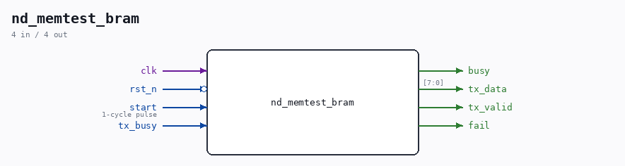
| Direction | Width | Name | Description |
|---|---|---|---|
| input | 1 |
clk |
|
| input | 1 |
rst_n (active low) |
|
| input | 1 |
start |
1-cycle pulse |
| output | 1 |
busy |
|
| output | [7:0] |
tx_data |
|
| output | 1 |
tx_valid |
|
| input | 1 |
tx_busy |
|
| output | 1 |
fail |
Verilog source
Verilog/fpga/nexys4ddr/sd-fat-test/nd_memtest_bram.v on GitHub.
Show the Verilog of nd_memtest_bram (292 lines)
/****************************************************************************
** ND-120 memory-path test as a character stream                           **
**                                                                         **
** Same test as fpga/basys3/mem-test/basys3_mem_test_top.v - it isolates   **
** MEM_RAM_49 (-> SIP1M9 sync BRAM, ramSize=3) from the whole CPU and      **
** drives the EXACT DRAM RAS/CAS/AA protocol the real controller uses      **
** (measured via DBG_MEM: row valid at RAS fall, AA -> column while CAS is **
** still high, both strobes low a few cycles, read data captured while RAS **
** is deasserted and CAS still low), then writes, reads back and verifies  **
** a set of addresses.                                                     **
**                                                                         **
** The difference from the Basys3 version is only the OUTPUT: that one     **
** owns a UART, this one emits bytes through a tx_data/tx_valid/tx_busy    **
** handshake so it can be a command inside the SD-FAT test menu and share  **
** that design's UART.                                                     **
**                                                                         **
** Same vectors as the Basys3 run, so the two boards are directly          **
** comparable: if this PASSES the ND-120 BRAM memory path is sound and a   **
** memory fault lives in the CPU/MAC integration; if it FAILS the fault is **
** here, where it can be iterated on without the CPU in the way.           **
**                                                                         **
** Report (one line per vector, then a verdict):                           **
**   NDMEM START                                                           **
**   ND 00000 W A5 R A5 OK                                                 **
**   ...                                                                   **
**   NDMEM PASS   (or NDMEM FAIL n)                                        **
**                                                                         **
** Last reviewed: 20-AUG-2026                                              **
** Ronny Hansen                                                            **
*****************************************************************************/
`default_nettype none

module nd_memtest_bram (
    input wire clk,
    input wire rst_n,

    input  wire start,  // 1-cycle pulse
    output wire busy,

    // character output, arbitrated by the caller
    output reg [7:0] tx_data,
    output reg       tx_valid,
    input  wire      tx_busy,

    output reg fail
);

  /*******************************************************************
   *  The sheet-49 RAM under test
   *******************************************************************/
  reg  [ 9:0] aa;
  reg         ras, cas, bank0, mwrite_n;
  reg  [17:0] dd_in;
  wire [17:0] dd_out;
  wire        corr_n;

  MEM_RAM_49 ram (
      .sysclk(clk),
      .sys_rst_n(rst_n),
      .AA_9_0(aa),
      .BANK0(bank0),
      .BANK1(1'b0),
      .BANK2(1'b0),
      .CAS(cas),
      .RAS(ras),
      .MWRITE50_n(mwrite_n),
      .DD_17_0_IN(dd_in),
      .DD_17_0_OUT(dd_out),
      .CORR_n(corr_n)
  );

  /*******************************************************************
   *  Test vectors - identical to the Basys3 mem-test
   *******************************************************************/
  reg [19:0] t_addr;
  reg [ 7:0] t_data;
  reg [ 2:0] tidx;
  always @(*) begin
    case (tidx)
      3'd0: begin t_addr = 20'h00000; t_data = 8'hA5; end
      3'd1: begin t_addr = 20'h00001; t_data = 8'h5A; end
      3'd2: begin t_addr = 20'h00002; t_data = 8'h3C; end
      3'd3: begin t_addr = 20'h00004; t_data = 8'hC3; end  // old model aliased 0<->4
      3'd4: begin t_addr = 20'h00010; t_data = 8'hFF; end
      3'd5: begin t_addr = 20'h00100; t_data = 8'h11; end
      3'd6: begin t_addr = 20'h000FF; t_data = 8'h77; end
      3'd7: begin t_addr = 20'h003FF; t_data = 8'h42; end
    endcase
  end
  wire [9:0] row = t_addr[9:0];
  wire [9:0] col = t_addr[19:10];

  /*******************************************************************
   *  Line assembler: build up to 32 characters, then shift them out
   *******************************************************************/
  reg [7:0] line[0:31];
  reg [5:0] line_len;
  reg [5:0] line_ptr;
  reg       emitting;

  function [7:0] hexch;
    input [3:0] v;
    begin
      hexch = (v < 4'd10) ? (8'h30 + {4'b0, v}) : (8'h41 + {4'b0, (v - 4'd10)});
    end
  endfunction

  /*******************************************************************
   *  Main FSM
   *******************************************************************/
  localparam S_IDLE   = 4'd0;
  localparam S_BANNER = 4'd1;
  localparam S_WR     = 4'd2;
  localparam S_RD     = 4'd3;
  localparam S_LINE   = 4'd4;
  localparam S_EMIT   = 4'd5;
  localparam S_NEXT   = 4'd6;
  localparam S_RESULT = 4'd7;
  localparam S_END    = 4'd8;

  reg [3:0] state;
  reg [3:0] d;  // DRAM sub-cycle 0..6
  reg [7:0] rd_data;
  reg [2:0] nfail;
  reg [3:0] after_emit;

  assign busy = (state != S_IDLE);

  // DRAM protocol driven by sub-cycle d (each = one clk), exactly as measured.
  // Non-blocking throughout (the Basys3 original mixes blocking and
  // non-blocking, which Verilator rejects outright): each arm writes the
  // defaults first and then overrides, and the last non-blocking write to a
  // signal in a timestep is the one that lands, so the behaviour is the same.
  task drive_dram(input is_write);
    begin
      ras <= 1'b0; cas <= 1'b0; bank0 <= 1'b0; mwrite_n <= 1'b1;
      aa <= row; dd_in <= {10'b0, t_data};
      case (d)
        4'd0: begin ras <= 1; bank0 <= 1; aa <= row; mwrite_n <= is_write?1'b0:1'b1; end  // RAS fall, row
        4'd1: begin ras <= 1; bank0 <= 1; aa <= col; mwrite_n <= is_write?1'b0:1'b1; end  // AA -> column
        4'd2: begin ras <= 1; bank0 <= 1; cas <= 1; aa <= col; mwrite_n <= is_write?1'b0:1'b1; end  // CAS fall
        4'd3: begin ras <= 1; bank0 <= 1; cas <= 1; aa <= col; mwrite_n <= is_write?1'b0:1'b1; end  // both low
        4'd4: begin ras <= 1; bank0 <= 1; cas <= 1; aa <= col; mwrite_n <= is_write?1'b0:1'b1; end  // both low
        4'd5: begin ras <= 0; bank0 <= 1; cas <= 1; aa <= col; mwrite_n <= 1'b1; end          // read window
        default: begin ras <= 0; cas <= 0; bank0 <= 0; end                             // precharge
      endcase
    end
  endtask

  integer i;

  always @(posedge clk) begin
    if (!rst_n) begin
      state    <= S_IDLE;
      d        <= 4'd0;
      tidx     <= 3'd0;
      fail     <= 1'b0;
      nfail    <= 3'd0;
      tx_valid <= 1'b0;
      emitting <= 1'b0;
      line_len <= 6'd0;
      line_ptr <= 6'd0;
      rd_data  <= 8'd0;
      ras      <= 1'b0;
      cas      <= 1'b0;
      bank0    <= 1'b0;
      mwrite_n <= 1'b1;
      aa       <= 10'd0;
      dd_in    <= 18'd0;
    end else begin
      tx_valid <= 1'b0;

      case (state)
        S_IDLE:
        if (start) begin
          fail  <= 1'b0;
          nfail <= 3'd0;
          tidx  <= 3'd0;
          d     <= 4'd0;
          state <= S_BANNER;
        end

        // "NDMEM START" CR LF
        S_BANNER: begin
          line[0]  <= "N"; line[1] <= "D"; line[2] <= "M"; line[3] <= "E";
          line[4]  <= "M"; line[5] <= " "; line[6] <= "S"; line[7] <= "T";
          line[8]  <= "A"; line[9] <= "R"; line[10] <= "T";
          line[11] <= 8'h0D; line[12] <= 8'h0A;
          line_len <= 6'd13;
          line_ptr <= 6'd0;
          after_emit <= S_WR;
          d <= 4'd0;
          state <= S_EMIT;
        end

        S_WR: begin
          drive_dram(1'b1);
          if (d == 4'd6) begin d <= 4'd0; state <= S_RD; end
          else d <= d + 4'd1;
        end

        S_RD: begin
          drive_dram(1'b0);
          if (d == 4'd5) rd_data <= dd_out[7:0];  // capture in the read window
          if (d == 4'd6) begin d <= 4'd0; state <= S_LINE; end
          else d <= d + 4'd1;
        end

        // "ND aaaaa W dd R dd OK" CR LF
        S_LINE: begin
          line[0]  <= "N"; line[1] <= "D"; line[2] <= " ";
          line[3]  <= hexch(t_addr[19:16]);
          line[4]  <= hexch(t_addr[15:12]);
          line[5]  <= hexch(t_addr[11:8]);
          line[6]  <= hexch(t_addr[7:4]);
          line[7]  <= hexch(t_addr[3:0]);
          line[8]  <= " "; line[9] <= "W"; line[10] <= " ";
          line[11] <= hexch(t_data[7:4]);
          line[12] <= hexch(t_data[3:0]);
          line[13] <= " "; line[14] <= "R"; line[15] <= " ";
          line[16] <= hexch(rd_data[7:4]);
          line[17] <= hexch(rd_data[3:0]);
          line[18] <= " ";
          if (rd_data == t_data) begin
            line[19] <= "O"; line[20] <= "K";
          end else begin
            line[19] <= "E"; line[20] <= "R";
            fail  <= 1'b1;
            nfail <= nfail + 3'd1;
          end
          line[21] <= 8'h0D; line[22] <= 8'h0A;
          line_len <= 6'd23;
          line_ptr <= 6'd0;
          after_emit <= S_NEXT;
          state <= S_EMIT;
        end

        // shift the assembled line out through the tx handshake
        S_EMIT:
        if (!tx_busy && !tx_valid) begin
          if (line_ptr == line_len) begin
            state <= after_emit;
          end else begin
            tx_data  <= line[line_ptr[4:0]];
            tx_valid <= 1'b1;
            line_ptr <= line_ptr + 6'd1;
          end
        end

        S_NEXT:
        if (tidx == 3'd7) state <= S_RESULT;
        else begin
          tidx  <= tidx + 3'd1;
          d     <= 4'd0;
          state <= S_WR;
        end

        // "NDMEM PASS" / "NDMEM FAIL n"
        S_RESULT: begin
          line[0] <= "N"; line[1] <= "D"; line[2] <= "M"; line[3] <= "E";
          line[4] <= "M"; line[5] <= " ";
          if (!fail) begin
            line[6]  <= "P"; line[7] <= "A"; line[8] <= "S"; line[9] <= "S";
            line[10] <= 8'h0D; line[11] <= 8'h0A;
            line_len <= 6'd12;
          end else begin
            line[6]  <= "F"; line[7] <= "A"; line[8] <= "I"; line[9] <= "L";
            line[10] <= " ";
            line[11] <= 8'h30 + {5'b0, nfail};
            line[12] <= 8'h0D; line[13] <= 8'h0A;
            line_len <= 6'd14;
          end
          line_ptr   <= 6'd0;
          after_emit <= S_END;
          state      <= S_EMIT;
        end

        S_END: begin
          ras   <= 1'b0;
          cas   <= 1'b0;
          bank0 <= 1'b0;
          state <= S_IDLE;
        end

        default: state <= S_IDLE;
      endcase
    end
  end

endmodule

`default_nettype wire