nd_ddr2_storage
Source: Verilog/fpga/nexys4ddr/ddr2/nd_ddr2_storage.v
Where it sits (Nexys): nd120_nexys4ddr_top > nd_ddr2_storage
- instance path: u_region
Used in: nd120_nexys4ddr_top (Nexys)
Contains: no other modules.
Module hierarchy - All modules
Schematic
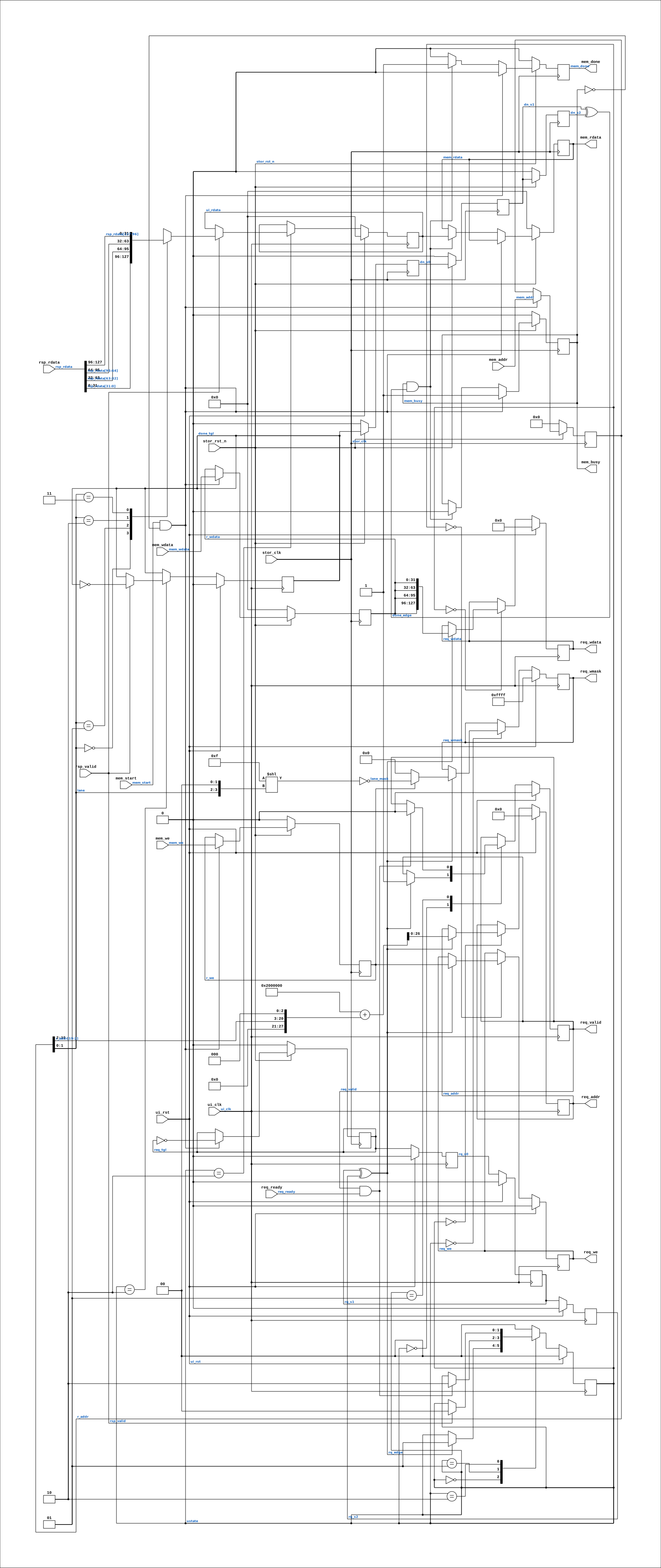
Drawn from the Verilog: the yosys netlist of the Nexys 4 DDR build, instance u_region. Sub-modules are boxes (click the picture to open it full size; there every sub-module box links to its page, and every wire shows its Verilog name).
Description
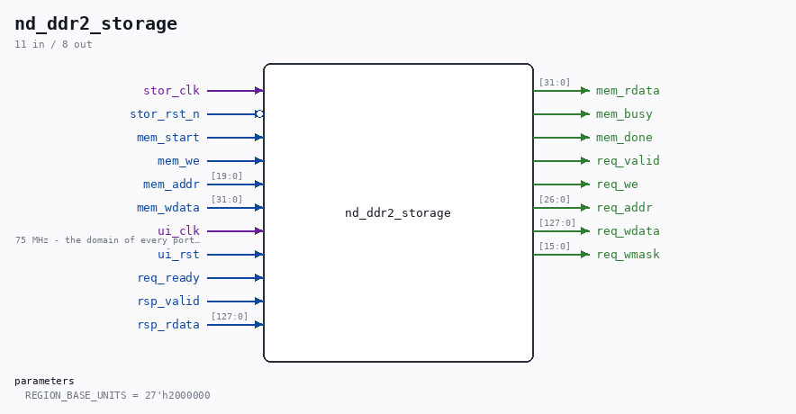
nd_ddr2_storage - the nd_storage region, held in DDR2 nd_storage keeps a REGION of block storage that its Phase-4 tag directory uses as a CACHE of the disc images on the SD card (Verilog/SD-FAT/circuit/nd_storage_cache.v): the disc classes are cached, tape and floppy go direct to the card, and writes go through to the card. On the Tang Nano 20K that region lives in the upper half of the single SDRAM chip, reached through MEM_RAM_49_SDRAM's ND_STORAGE_PORT because the CPU's main memory shares the same chip. This board has DDR2 that nothing else uses yet, so the region connects to it DIRECTLY through ../ddr2/nd_ddr2_port.v - no detour through the CPU memory path. When ND-120 main memory later moves into DDR2 as well, nd_ddr2_port is the place that arbitrates the two clients. THE PORT CONTRACT (from nd_storage_engine.v, matched exactly): mem_start 1-cycle pulse, only legal while mem_busy = 0 mem_we / mem_addr / mem_wdata stable from mem_start until mem_done mem_rdata valid at mem_done and held afterwards mem_busy level, high for the whole operation mem_done 1-cycle pulse ADDRESS MAPPING mem_addr[19:0] indexes 32-bit words: 1M words = 4 MB of region. One DDR2 transfer is 128 bits = four of those words, and app_addr counts 16-bit units with 8 units per transfer, so: transfer index = mem_addr[19:2] word in transfer = mem_addr[1:0] req_addr = REGION_BASE_UNITS + {mem_addr[19:2], 3'b000} A write updates ONE 32-bit word, so it uses the byte mask rather than a read-modify-write: MIG's mask is active low, so the four bytes of the selected lane are 0 and the other twelve are 1. CLOCK DOMAINS: the storage stack runs on stor_clk (27 MHz here), the controller on ui_clk (75 MHz). The request crosses as a toggle with the payload held stable behind it, and completion comes back as a second toggle - the same shape MEM_RAM_49_SDRAM uses on the Tang. Last reviewed: 20-AUG-2026 Ronny Hansen
Parameters
| Parameter | Default |
|---|---|
REGION_BASE_UNITS |
27'h2000000 |
Ports
| Direction | Width | Name | Description |
|---|---|---|---|
| input | 1 |
stor_clk |
|
| input | 1 |
stor_rst_n (active low) |
|
| input | 1 |
mem_start |
|
| input | 1 |
mem_we |
|
| input | [19:0] |
mem_addr |
|
| input | [31:0] |
mem_wdata |
|
| output | [31:0] |
mem_rdata |
|
| output | 1 |
mem_busy |
|
| output | 1 |
mem_done |
|
| input | 1 |
ui_clk |
75 MHz - the domain of every port signal below (from nd_ddr2_port.ui_clk) |
| input | 1 |
ui_rst |
|
| output | 1 |
req_valid |
|
| output | 1 |
req_we |
|
| output | [26:0] |
req_addr |
|
| output | [127:0] |
req_wdata |
|
| output | [15:0] |
req_wmask |
|
| input | 1 |
req_ready |
|
| input | 1 |
rsp_valid |
|
| input | [127:0] |
rsp_rdata |
Verilog source
Verilog/fpga/nexys4ddr/ddr2/nd_ddr2_storage.v on GitHub.
Show the Verilog of nd_ddr2_storage (192 lines)
/****************************************************************************
** nd_ddr2_storage - the nd_storage region, held in DDR2                    **
**                                                                         **
** nd_storage keeps a REGION of block storage that its Phase-4 tag          **
** directory uses as a CACHE of the disc images on the SD card              **
** (Verilog/SD-FAT/circuit/nd_storage_cache.v): the disc classes are        **
** cached, tape and floppy go direct to the card, and writes go through to  **
** the card. On the Tang Nano 20K that region lives in the upper half of    **
** the single SDRAM chip, reached through MEM_RAM_49_SDRAM's                **
** ND_STORAGE_PORT because the CPU's main memory shares the same chip.      **
**                                                                         **
** This board has DDR2 that nothing else uses yet, so the region connects   **
** to it DIRECTLY through ../ddr2/nd_ddr2_port.v - no detour through the    **
** CPU memory path. When ND-120 main memory later moves into DDR2 as well,  **
** nd_ddr2_port is the place that arbitrates the two clients.               **
**                                                                         **
** THE PORT CONTRACT (from nd_storage_engine.v, matched exactly):           **
**   mem_start  1-cycle pulse, only legal while mem_busy = 0                **
**   mem_we / mem_addr / mem_wdata  stable from mem_start until mem_done    **
**   mem_rdata  valid at mem_done and held afterwards                       **
**   mem_busy   level, high for the whole operation                         **
**   mem_done   1-cycle pulse                                               **
**                                                                         **
** ADDRESS MAPPING                                                          **
**   mem_addr[19:0] indexes 32-bit words: 1M words = 4 MB of region.        **
**   One DDR2 transfer is 128 bits = four of those words, and app_addr      **
**   counts 16-bit units with 8 units per transfer, so:                     **
**       transfer index = mem_addr[19:2]                                    **
**       word in transfer = mem_addr[1:0]                                   **
**       req_addr = REGION_BASE_UNITS + {mem_addr[19:2], 3'b000}            **
**   A write updates ONE 32-bit word, so it uses the byte mask rather than  **
**   a read-modify-write: MIG's mask is active low, so the four bytes of    **
**   the selected lane are 0 and the other twelve are 1.                    **
**                                                                         **
** CLOCK DOMAINS: the storage stack runs on stor_clk (27 MHz here), the     **
** controller on ui_clk (75 MHz). The request crosses as a toggle with the  **
** payload held stable behind it, and completion comes back as a second     **
** toggle - the same shape MEM_RAM_49_SDRAM uses on the Tang.               **
**                                                                         **
** Last reviewed: 20-AUG-2026                                              **
** Ronny Hansen                                                            **
*****************************************************************************/
`default_nettype none

module nd_ddr2_storage #(
    // Where the region sits in DDR2, in 16-bit units. Default 64 MiB in, so
    // the bottom half of the device stays free for ND-120 main memory later.
    parameter [26:0] REGION_BASE_UNITS = 27'h2000000
) (
    // ---- storage side (stor_clk) ----
    input  wire        stor_clk,
    input  wire        stor_rst_n,
    input  wire        mem_start,
    input  wire        mem_we,
    input  wire [19:0] mem_addr,
    input  wire [31:0] mem_wdata,
    output reg  [31:0] mem_rdata,
    output wire        mem_busy,
    output reg         mem_done,

    // ---- controller side (ui_clk), wired to nd_ddr2_port ----
    input  wire          ui_clk,  //! 75 MHz - the domain of every port signal below (from nd_ddr2_port.ui_clk)
    input  wire          ui_rst,
    output reg           req_valid,
    output reg           req_we,
    output reg  [ 26:0]  req_addr,
    output reg  [127:0]  req_wdata,
    output reg  [ 15:0]  req_wmask,
    input  wire          req_ready,
    input  wire          rsp_valid,
    input  wire [127:0]  rsp_rdata
);

  /*******************************************************************
   *  stor_clk side: latch the request, raise busy, flip the toggle
   *******************************************************************/
  reg        busy_r;
  reg        req_tgl;
  reg        r_we;
  reg [19:0] r_addr;
  reg [31:0] r_wdata;

  assign mem_busy = busy_r;

  // completion toggle coming back from ui_clk
  reg dn_s0, dn_s1, dn_s2;
  always @(posedge stor_clk) begin
    if (!stor_rst_n) begin dn_s0 <= 1'b0; dn_s1 <= 1'b0; dn_s2 <= 1'b0; end
    else begin dn_s0 <= done_tgl; dn_s1 <= dn_s0; dn_s2 <= dn_s1; end
  end
  wire done_edge = dn_s1 ^ dn_s2;

  always @(posedge stor_clk) begin
    if (!stor_rst_n) begin
      busy_r    <= 1'b0;
      req_tgl   <= 1'b0;
      mem_done  <= 1'b0;
      mem_rdata <= 32'd0;
      r_we      <= 1'b0;
      r_addr    <= 20'd0;
      r_wdata   <= 32'd0;
    end else begin
      mem_done <= 1'b0;

      if (mem_start && !busy_r) begin
        r_we    <= mem_we;
        r_addr  <= mem_addr;
        r_wdata <= mem_wdata;
        busy_r  <= 1'b1;
        req_tgl <= ~req_tgl;
      end else if (busy_r && done_edge) begin
        // ui_rdata was captured several ui_clk cycles before the toggle
        // flipped, so it is stable to sample here
        mem_rdata <= ui_rdata;
        mem_done  <= 1'b1;
        busy_r    <= 1'b0;
      end
    end
  end

  /*******************************************************************
   *  ui_clk side: run one DDR2 transfer per request toggle
   *******************************************************************/
  reg        done_tgl;
  reg [31:0] ui_rdata;

  reg rq_s0, rq_s1, rq_s2;
  always @(posedge ui_clk) begin
    if (ui_rst) begin rq_s0 <= 1'b0; rq_s1 <= 1'b0; rq_s2 <= 1'b0; end
    else begin rq_s0 <= req_tgl; rq_s1 <= rq_s0; rq_s2 <= rq_s1; end
  end
  wire rq_edge = rq_s1 ^ rq_s2;

  // r_we / r_addr / r_wdata are held stable by the contract from the start
  // pulse until done, so they are safe to sample here once the toggle lands
  wire [1:0]  lane = r_addr[1:0];
  wire [15:0] lane_mask = ~(16'h000F << {lane, 2'b00});

  localparam U_IDLE = 2'd0;
  localparam U_REQ  = 2'd1;
  localparam U_WAIT = 2'd2;

  reg [1:0] ustate;

  always @(posedge ui_clk) begin
    if (ui_rst) begin
      ustate    <= U_IDLE;
      req_valid <= 1'b0;
      req_we    <= 1'b0;
      req_addr  <= 27'd0;
      req_wdata <= 128'd0;
      req_wmask <= 16'hFFFF;
      done_tgl  <= 1'b0;
      ui_rdata  <= 32'd0;
    end else begin
      case (ustate)
        U_IDLE:
        if (rq_edge) begin
          req_we    <= r_we;
          req_addr  <= REGION_BASE_UNITS + {7'd0, r_addr[19:2], 3'b000};
          req_wdata <= {4{r_wdata}};        // the mask picks the live lane
          req_wmask <= r_we ? lane_mask : 16'h0000;
          req_valid <= 1'b1;
          ustate    <= U_REQ;
        end

        U_REQ:
        if (req_valid && req_ready) begin
          req_valid <= 1'b0;   // dropped in the cycle it is accepted
          ustate    <= U_WAIT;
        end

        U_WAIT:
        if (rsp_valid) begin
          case (lane)
            2'd0: ui_rdata <= rsp_rdata[31:0];
            2'd1: ui_rdata <= rsp_rdata[63:32];
            2'd2: ui_rdata <= rsp_rdata[95:64];
            2'd3: ui_rdata <= rsp_rdata[127:96];
          endcase
          done_tgl <= ~done_tgl;
          ustate   <= U_IDLE;
        end

        default: ustate <= U_IDLE;
      endcase
    end
  end

endmodule

`default_nettype wire