PAL_44446B_D
Source: Verilog/CPU-BOARD-3202/circuit/PAL_44446B_D.v
Where it sits (Simulation): ND120_TOP > ND120_CORE > ND3202D > MEM_43 > MEM_ADEC_45 > PAL_44446B_D
- instance path: CORE.CPU_BOARD.MEM.ADEC.PAL_UBADEC
Used in: MEM_ADEC_45 (all tops)
Contains: no other modules.
Module hierarchy - All modules
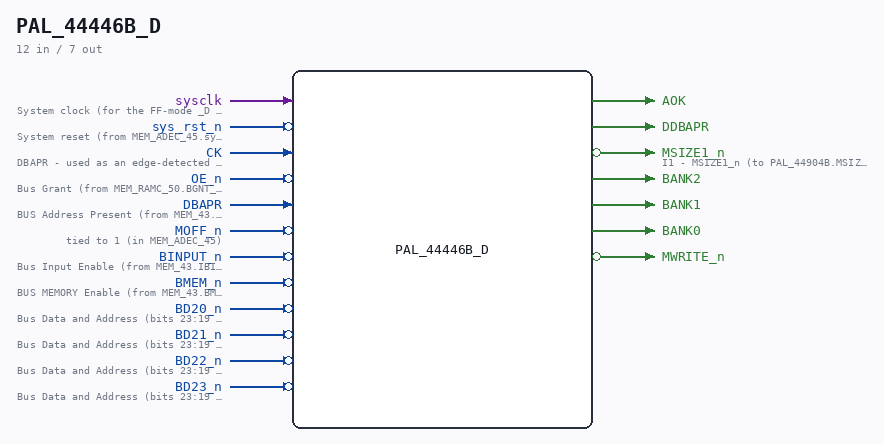
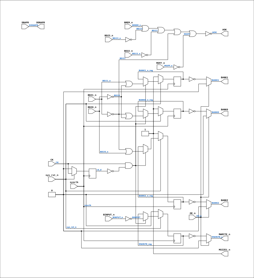
Schematic
Drawn from the Verilog: the yosys netlist of the Simulation (Verilator) build, instance CORE.CPU_BOARD.MEM.ADEC.PAL_UBADEC. Sub-modules are boxes (click the picture to open it full size; there every sub-module box links to its page, and every wire shows its Verilog name).
Description
PAL_44446B_D - sysclk-domain mirror of PAL_44446B (UBADEC) Same equations; the four registers sample on sysclk with a rising- edge ENABLE on the original CK (DBAPR) instead of using it as a clock net (routed-net-as-clock breaks the write phase on FPGA - see docs/nd120-dram-memory.md section 5). PAL file itself untouched. Pattern: CYC_CC_D / CYC_TERM_D. Last reviewed: 8-JUL-2026 Ronny Hansen
Ports
| Direction | Width | Name | Description |
|---|---|---|---|
| input | 1 |
sysclk |
System clock (for the FF-mode _D PAL mirrors) (from MEM_ADEC_45.sysclk) |
| input | 1 |
sys_rst_n (active low) |
System reset (from MEM_ADEC_45.sys_rst_n) |
| input | 1 |
CK |
DBAPR - used as an edge-detected ENABLE here |
| input | 1 |
OE_n (active low) |
Bus Grant (from MEM_RAMC_50.BGNT_n) |
| input | 1 |
DBAPR |
BUS Address Present (from MEM_43.DBAPR) |
| input | 1 |
MOFF_n (active low) |
tied to 1 (in MEM_ADEC_45) |
| input | 1 |
BINPUT_n (active low) |
Bus Input Enable (from MEM_43.IBINPUT_n) |
| input | 1 |
BMEM_n (active low) |
BUS MEMORY Enable (from MEM_43.BMEM_n) |
| input | 1 |
BD20_n (active low) |
Bus Data and Address (bits 23:19 negated) (from MEM_43.BD_23_19_n[1]) |
| input | 1 |
BD21_n (active low) |
Bus Data and Address (bits 23:19 negated) (from MEM_43.BD_23_19_n[2]) |
| input | 1 |
BD22_n (active low) |
Bus Data and Address (bits 23:19 negated) (from MEM_43.BD_23_19_n[3]) |
| input | 1 |
BD23_n (active low) |
Bus Data and Address (bits 23:19 negated) (from MEM_43.BD_23_19_n[4]) |
| output | 1 |
AOK |
|
| output | 1 |
DDBAPR |
|
| output | 1 |
MSIZE1_n (active low) |
I1 - MSIZE1_n (to PAL_44904B.MSIZE1_n) |
| output | 1 |
BANK2 |
|
| output | 1 |
BANK1 |
|
| output | 1 |
BANK0 |
|
| output | 1 |
MWRITE_n (active low) |
Verilog source
Verilog/CPU-BOARD-3202/circuit/PAL_44446B_D.v on GitHub.
Show the Verilog of PAL_44446B_D (64 lines)
/**************************************************************************
** PAL_44446B_D - sysclk-domain mirror of PAL_44446B (UBADEC)            **
** Same equations; the four registers sample on sysclk with a rising-    **
** edge ENABLE on the original CK (DBAPR) instead of using it as a       **
** clock net (routed-net-as-clock breaks the write phase on FPGA -       **
** see docs/nd120-dram-memory.md section 5). PAL file itself untouched.  **
** Pattern: CYC_CC_D / CYC_TERM_D.                                       **
** Last reviewed: 8-JUL-2026  Ronny Hansen                               **
***************************************************************************/
module PAL_44446B_D (
    input sysclk,    //! System clock (for the FF-mode _D PAL mirrors) (from MEM_ADEC_45.sysclk)
    input sys_rst_n,  //! System reset (from MEM_ADEC_45.sys_rst_n)
    input CK,        // DBAPR - used as an edge-detected ENABLE here
    input OE_n,      //! Bus Grant (from MEM_RAMC_50.BGNT_n)
    input DBAPR,     //! BUS Address Present (from MEM_43.DBAPR)
    input MOFF_n,    //! tied to 1 (in MEM_ADEC_45)
    input BINPUT_n,  //! Bus Input Enable (from MEM_43.IBINPUT_n)
    input BMEM_n,    //! BUS MEMORY Enable (from MEM_43.BMEM_n)
    input BD20_n,    //! Bus Data and Address (bits 23:19 negated) (from MEM_43.BD_23_19_n[1])
    input BD21_n,    //! Bus Data and Address (bits 23:19 negated) (from MEM_43.BD_23_19_n[2])
    input BD22_n,    //! Bus Data and Address (bits 23:19 negated) (from MEM_43.BD_23_19_n[3])
    input BD23_n,    //! Bus Data and Address (bits 23:19 negated) (from MEM_43.BD_23_19_n[4])
    output AOK,
    output DDBAPR,
    output MSIZE1_n,  //! I1 - MSIZE1_n (to PAL_44904B.MSIZE1_n)
    output BANK2,
    output BANK1,
    output BANK0,
    output MWRITE_n
);
  wire BD20 = ~BD20_n;
  wire BD21 = ~BD21_n;
  wire BD22 = ~BD22_n;
  wire BD23 = ~BD23_n;
  wire MOFF = ~MOFF_n;
  wire BINPUT = ~BINPUT_n;

  reg BANK0_n_reg, BANK1_n_reg, BANK2_n_reg, MWRITE_reg;
  reg ck_d;
  always @(posedge sysclk) begin
    if (!sys_rst_n) begin
      ck_d <= 0;
      BANK0_n_reg <= 1; BANK1_n_reg <= 1; BANK2_n_reg <= 1;
      MWRITE_reg <= 0;
    end else begin
      ck_d <= CK;
      if (CK && !ck_d) begin  // one capture per CK (DBAPR) rise
        BANK0_n_reg <= BD21 | BD20;
        BANK2_n_reg <= BD21 | BD20_n;
        BANK1_n_reg <= BD21_n | BD20;
        MWRITE_reg  <= BINPUT;
      end
    end
  end

  assign BANK2 = OE_n ? 1'b0 : ~BANK2_n_reg;
  assign BANK1 = OE_n ? 1'b0 : ~BANK1_n_reg;
  assign BANK0 = OE_n ? 1'b0 : ~BANK0_n_reg;
  assign MWRITE_n = OE_n ? 1'b0 : ~MWRITE_reg;

  assign AOK = ~(BMEM_n | BD23 | BD22 | BD21 | MOFF);
  assign DDBAPR = DBAPR;
  assign MSIZE1_n = 1;
endmodule