CPU_CS_PROM_19
Source: Verilog/CPU-BOARD-3202/circuit/CPU_CS_PROM_19.v
Where it sits (Simulation): ND120_TOP > ND120_CORE > ND3202D > CPU_15 > CPU_CS_16 > CPU_CS_PROM_19
- instance path: CORE.CPU_BOARD.CPU.CS.PROM
Used in: CPU_CS_16 (all tops)
Contains: no other modules.
Module hierarchy - All modules
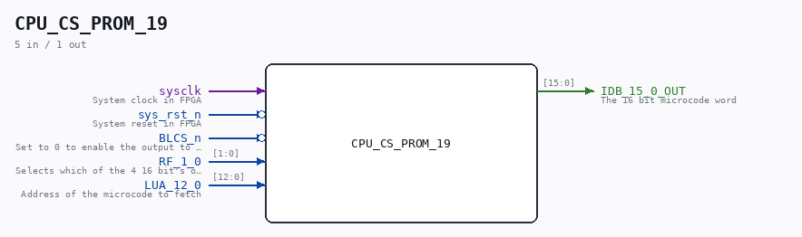
Schematic
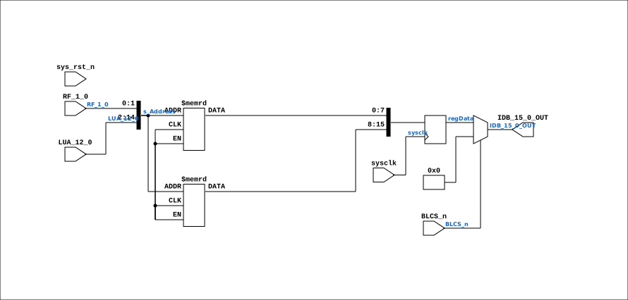
Drawn from the Verilog: the yosys netlist of the Simulation (Verilator) build, instance CORE.CPU_BOARD.CPU.CS.PROM. Sub-modules are boxes (click the picture to open it full size; there every sub-module box links to its page, and every wire shows its Verilog name).
Description
ND120 CPU, MM&M CPU/CS/PROM PROMS SHEET 19 of 50 Last reviewed: 9-FEB-2025 Ronny Hansen
Ports
| Direction | Width | Name | Description |
|---|---|---|---|
| input | 1 |
sysclk |
System clock in FPGA |
| input | 1 |
sys_rst_n (active low) |
System reset in FPGA |
| input | 1 |
BLCS_n (active low) |
Set to 0 to enable the output to IDB |
| input | [1:0] |
RF_1_0 |
Selects which of the 4 16 bit's of the microcoe to fetch |
| input | [12:0] |
LUA_12_0 |
Address of the microcode to fetch |
| output | [15:0] |
IDB_15_0_OUT |
The 16 bit microcode word |
Verilog source
Verilog/CPU-BOARD-3202/circuit/CPU_CS_PROM_19.v on GitHub.
Show the Verilog of CPU_CS_PROM_19 (81 lines)
/**************************************************************************
** ND120 CPU, MM&M                                                       **
** CPU/CS/PROM                                                           **
** PROMS                                                                 **
** SHEET 19 of 50                                                        **
**                                                                       **
** Last reviewed: 9-FEB-2025                                             **
** Ronny Hansen                                                          **
***************************************************************************/

//`define GOWIN // Uncomment this for Gowin platform

module CPU_CS_PROM_19 (
  // System Input signals
  input sysclk,    //! System clock in FPGA
  input sys_rst_n, //! System reset in FPGA

    // Input signals
  input        BLCS_n,   // Set to 0 to enable the output to IDB
  input [ 1:0] RF_1_0,   // Selects which of the 4 16 bit's of the microcoe to fetch
  input [12:0] LUA_12_0, // Address of the microcode to fetch

  output [15:0] IDB_15_0_OUT  // The 16 bit microcode word
);


  wire [14:0] s_Address;
  (* mark_debug = "true", DONT_TOUCH = "true" *) reg [15:0] regData;

  assign s_Address = {LUA_12_0, RF_1_0};  // Concatenate the bits to form a 15-bit address

  // AM27256_45132L = Contains the LO 8 bits (0-7) AM27256_45133L = Contains the HI 8 bits (8-15)

  // Drop the microcode ROM arrays entirely when they are never read:
  //  - GOWIN         : Tang Nano 20K loads microcode via SKIP_WCS_LOAD; no ROM path.
  //  - SKIP_WCS_LOAD : the WCS is bitstream-preloaded, so the PROM->WCS runtime load
  //                    never runs and this PROM is dead. On Xilinx this reclaims the
  //                    ~7850 LUTs / BRAM the ROM would otherwise consume.
  // The Verilog preprocessor has no `||`, so fold both triggers into one helper.
`ifdef GOWIN
  `define ND_DROP_PROM_ROM
`endif
`ifdef SKIP_WCS_LOAD
  `define ND_DROP_PROM_ROM
`endif

`ifdef ND_DROP_PROM_ROM

`else

  // Xilinx: ram_style forces BRAM inference for ROM
  // Gowin: syn_ramstyle for block RAM inference
  (* ram_style = "block", syn_ramstyle = "block_ram" *)
  reg [7:0] rom_lo[0:32767];  // 32K x 8 bit ROM (LO 8 bits)
  initial $readmemh("AM27256_45132L.hex", rom_lo);

  (* ram_style = "block", syn_ramstyle = "block_ram" *)
  reg [7:0] rom_hi[0:32767];  // 32K x 8 bit ROM (HI 8 bits)
  initial $readmemh("AM27256_45133L.hex", rom_hi);
`endif

  // Registered ROM read - single stage (1 cycle latency).
  // The microcode sequencer expects data 1 cycle after address.
  // NOTE: Vivado may map this to LUT ROM instead of BRAM.
  // That's OK -- correctness over BRAM savings.

  always @(posedge sysclk) begin
    `ifdef ND_DROP_PROM_ROM
      // ROM arrays removed (GOWIN or SKIP_WCS_LOAD): the PROM is never read.
      regData <= 0;
    `else
      regData[7:0]  <= rom_lo[s_Address];
      regData[15:8] <= rom_hi[s_Address];
    `endif
  end

  // Controlled Buffer
  assign IDB_15_0_OUT = (BLCS_n) ? 16'b0 : regData;


endmodule