MEM_RAM_49_SIM
Source: Verilog/CPU-BOARD-3202/circuit/MEM_RAM_49_SIM.v
Where it sits (Simulation): ND120_TOP > ND120_CORE > ND3202D > MEM_43 > MEM_RAM_49_SIM
- instance path: CORE.CPU_BOARD.MEM.RAM
Used in: MEM_43 (Simulation)
Contains: no other modules.
Module hierarchy - All modules
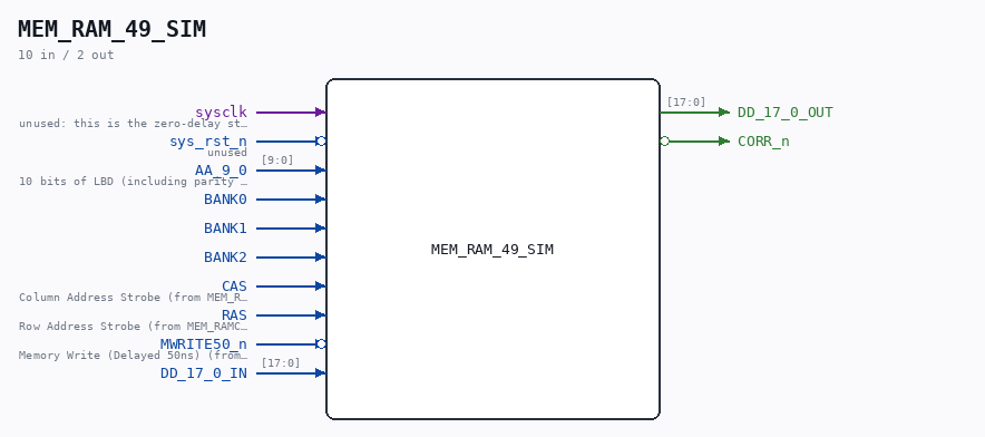
Schematic
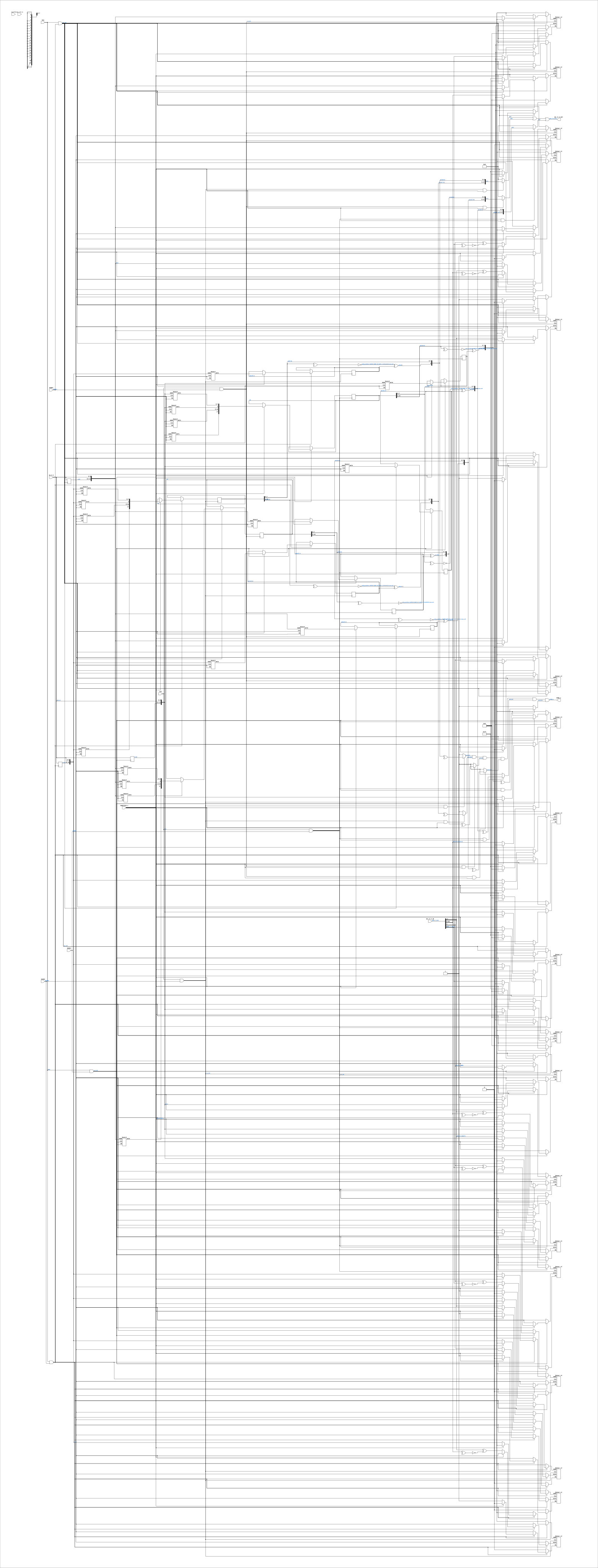
Drawn from the Verilog: the yosys netlist of the Simulation (Verilator) build, instance CORE.CPU_BOARD.MEM.RAM. Sub-modules are boxes (click the picture to open it full size; there every sub-module box links to its page, and every wire shows its Verilog name).
Description
ND120 CPU, MM&M MEM/RAM - Verilator simulation backend Drop-in replacement for the sheet-49 RAM (MEM_RAM_49): the original zero-delay DRAM model of the six SIP1M9 chips, ported to the shared sheet-49 interface. Selected automatically for VERILATOR_SIM builds (see MEM_43.v). Behavior is a faithful port of SIP1M9's ramSize=2 model: row latched on the (bank-gated) RAS edge, memory clocked on the (bank-gated) CAS edge, output gated by CAS, {row,col} indexing. Capacity: 3 banks x 1M x 18 bits = 6 MB, same as before. NOTE for the C++ harnesses (test_nd120.cpp / Run120.cpp / latch_ff_compare.cpp): programs are preloaded by poking the BANK0 arrays by hierarchical name: ...MEM__DOT__RAM__DOT__b0_lo [1M x 8] data bits 7:0 ...MEM__DOT__RAM__DOT__b0_lo_p [1M x 1] parity bit 8 ...MEM__DOT__RAM__DOT__b0_hi [1M x 8] data bits 16:9 ...MEM__DOT__RAM__DOT__b0_hi_p [1M x 1] parity bit 17 (same element widths as the old CHIP_15H/15J sdram/sdram_9 arrays). ND_SDRAM_PACK16: models the packed-storage memory contract of the Tang SDRAM backend (docs/nd120-parity-analysis.md section 6) at the reference level: parity bits are NOT read back from storage - DD[8]/ DD[17] are recomputed from the data on every read (odd parity), so a deliberately-bad-parity write is absorbed. Capacity/banking and the C++ preload hooks are unchanged (preload parity arrays become don't-cares on read). The physical packing/DQM layer itself is validated by the sdram-bridge tbs and the Tang full-boot vtest. Last reviewed: 11-JUL-2026 Ronny Hansen
Ports
| Direction | Width | Name | Description |
|---|---|---|---|
| input | 1 |
sysclk |
unused: this is the zero-delay strobe-clocked model |
| input | 1 |
sys_rst_n (active low) |
unused |
| input | [9:0] |
AA_9_0 |
10 bits of LBD (including parity in bit 10)- 10 bit input to MEM/RAM (from MEM_ADDR_44.AA_9_0) |
| input | 1 |
BANK0 |
|
| input | 1 |
BANK1 |
|
| input | 1 |
BANK2 |
|
| input | 1 |
CAS |
Column Address Strobe (from MEM_RAMC_50.CAS) |
| input | 1 |
RAS |
Row Address Strobe (from MEM_RAMC_50.RAS) |
| input | 1 |
MWRITE50_n (active low) |
Memory Write (Delayed 50ns) (from MEM_LBDIF_48.MWRITE50_n) |
| input | [17:0] |
DD_17_0_IN |
|
| output | [17:0] |
DD_17_0_OUT |
|
| output | 1 |
CORR_n (active low) |
Verilog source
Verilog/CPU-BOARD-3202/circuit/MEM_RAM_49_SIM.v on GitHub.
Show the Verilog of MEM_RAM_49_SIM (257 lines)
/**************************************************************************
** ND120 CPU, MM&M                                                       **
** MEM/RAM - Verilator simulation backend                                **
** Drop-in replacement for the sheet-49 RAM (MEM_RAM_49): the original   **
** zero-delay DRAM model of the six SIP1M9 chips, ported to the shared   **
** sheet-49 interface. Selected automatically for VERILATOR_SIM builds   **
** (see MEM_43.v). Behavior is a faithful port of SIP1M9's ramSize=2     **
** model: row latched on the (bank-gated) RAS edge, memory clocked on    **
** the (bank-gated) CAS edge, output gated by CAS, {row,col} indexing.   **
**                                                                       **
** Capacity: 3 banks x 1M x 18 bits = 6 MB, same as before.              **
**                                                                       **
** NOTE for the C++ harnesses (test_nd120.cpp / Run120.cpp /             **
** latch_ff_compare.cpp): programs are preloaded by poking the BANK0     **
** arrays by hierarchical name:                                          **
**   ...MEM__DOT__RAM__DOT__b0_lo    [1M x 8]  data bits 7:0             **
**   ...MEM__DOT__RAM__DOT__b0_lo_p  [1M x 1]  parity bit 8              **
**   ...MEM__DOT__RAM__DOT__b0_hi    [1M x 8]  data bits 16:9            **
**   ...MEM__DOT__RAM__DOT__b0_hi_p  [1M x 1]  parity bit 17             **
** (same element widths as the old CHIP_15H/15J sdram/sdram_9 arrays).   **
**                                                                       **
** ND_SDRAM_PACK16: models the packed-storage memory contract of the     **
** Tang SDRAM backend (docs/nd120-parity-analysis.md section 6) at the   **
** reference level: parity bits are NOT read back from storage - DD[8]/  **
** DD[17] are recomputed from the data on every read (odd parity), so a  **
** deliberately-bad-parity write is absorbed. Capacity/banking and the   **
** C++ preload hooks are unchanged (preload parity arrays become         **
** don't-cares on read). The physical packing/DQM layer itself is        **
** validated by the sdram-bridge tbs and the Tang full-boot vtest.       **
**                                                                       **
** Last reviewed: 11-JUL-2026                                            **
** Ronny Hansen                                                          **
***************************************************************************/

module MEM_RAM_49_SIM (
    // Input signals (sheet-49 interface, same as MEM_RAM_49)
    /* verilator lint_off UNUSEDSIGNAL */
    input sysclk,     // unused: this is the zero-delay strobe-clocked model
    input sys_rst_n,  // unused
    /* verilator lint_on UNUSEDSIGNAL */

    input [9:0] AA_9_0,  //! 10 bits of LBD (including parity in bit 10)- 10 bit input to MEM/RAM (from MEM_ADDR_44.AA_9_0)
    input       BANK0,
    input       BANK1,
    input       BANK2,

    input CAS,        //! Column Address Strobe (from MEM_RAMC_50.CAS)
    input RAS,        //! Row Address Strobe (from MEM_RAMC_50.RAS)

    input MWRITE50_n,  //! Memory Write (Delayed 50ns) (from MEM_LBDIF_48.MWRITE50_n)

    input  [17:0] DD_17_0_IN,
    output [17:0] DD_17_0_OUT,

    output CORR_n
);

  localparam integer DEPTH = 1048576;  // 1M words per bank

  // Bank 0 arrays - names/widths are load-bearing for the C++ preload hooks
  reg [7:0] b0_lo  [0:DEPTH-1];
  reg       b0_lo_p[0:DEPTH-1];
  reg [7:0] b0_hi  [0:DEPTH-1];
  reg       b0_hi_p[0:DEPTH-1];

  reg [7:0] b1_lo  [0:DEPTH-1];
  reg       b1_lo_p[0:DEPTH-1];
  reg [7:0] b1_hi  [0:DEPTH-1];
  reg       b1_hi_p[0:DEPTH-1];

  reg [7:0] b2_lo  [0:DEPTH-1];
  reg       b2_lo_p[0:DEPTH-1];
  reg [7:0] b2_hi  [0:DEPTH-1];
  reg       b2_hi_p[0:DEPTH-1];

  // Deliberate-corruption flags, one bit per byte lane. 1 = the parity bit
  // presented on this write did NOT match the data, i.e. an AM29833A
  // forced-error write (45008B TST armed by "TRR ECCR"). Everything else -
  // every ordinary write, and every location never written - leaves these 0.
  //
  // These exist so that parity can stay COMPUTED-ON-READ (Ronny's 3-AUG-2026
  // policy) while the ECC-simulate probe still works. Storing the parity bit
  // itself and reading it back would be wrong here: an untouched location
  // holds data 0 with a 0 parity array, but odd parity of a zero byte is 1,
  // so every word the machine had not yet written would report a parity
  // error. A flag defaults to "not corrupted" and has no such failure mode.
  // It also leaves the b*_p arrays and the C++ preload hooks in
  // sim/nd120_probe.cpp and runSim/Run120.cpp exactly as they were.
  reg       b0_lo_bad[0:DEPTH-1];
  reg       b0_hi_bad[0:DEPTH-1];
  reg       b1_lo_bad[0:DEPTH-1];
  reg       b1_hi_bad[0:DEPTH-1];
  reg       b2_lo_bad[0:DEPTH-1];
  reg       b2_hi_bad[0:DEPTH-1];

  // Bank-gated strobes: posedge (RAS & BANKx) is the same event as the old
  // negedge of the chips' s_ras_bX = ~(RAS & BANKx)
  wire ras_b0 = RAS & BANK0;
  wire cas_b0 = CAS & BANK0;
  wire ras_b1 = RAS & BANK1;
  wire cas_b1 = CAS & BANK1;
  wire ras_b2 = RAS & BANK2;
  wire cas_b2 = CAS & BANK2;

  reg [9:0] row0, row1, row2;
  reg [17:0] q0, q1, q2;
  reg qbad0_lo, qbad0_hi, qbad1_lo, qbad1_hi, qbad2_lo, qbad2_hi;

  // Odd parity, AM29833A convention (PAR low on ODD, high on EVEN)
  function automatic odd_par(input [7:0] d);
    odd_par = ~(^d);
  endfunction

`ifdef ND120_PARFLAG_TRACE
  // Diagnostic only: report the first flag-setting writes, so it can be MEASURED
  // whether anything other than an AM29833A forced-error write marks a location.
  integer par_seen = 0;
  task par_report(input integer bank, input [19:0] idx, input [17:0] d);
    begin
      if (par_seen < 40) begin
        par_seen = par_seen + 1;
        $display("PARFLAG bank=%0d idx=%0h data=%h par_lo=%b/%b par_hi=%b/%b",
                 bank, idx, d[17:0],
                 d[8],  odd_par(d[7:0]),
                 d[17], odd_par(d[16:9]));
      end
    end
  endtask
`endif

  always @(posedge ras_b0) row0 <= AA_9_0;
  always @(posedge ras_b1) row1 <= AA_9_0;
  always @(posedge ras_b2) row2 <= AA_9_0;

  // {row, col} indexing - identical to the old sip_address
  wire [19:0] idx0 = {row0, AA_9_0};
  wire [19:0] idx1 = {row1, AA_9_0};
  wire [19:0] idx2 = {row2, AA_9_0};

  always @(posedge cas_b0)
    if (ras_b0) begin
      if (MWRITE50_n) begin
        q0 <= {b0_hi_p[idx0], b0_hi[idx0], b0_lo_p[idx0], b0_lo[idx0]};
        qbad0_lo <= b0_lo_bad[idx0];
        qbad0_hi <= b0_hi_bad[idx0];
      end else begin
        {b0_hi_p[idx0], b0_hi[idx0], b0_lo_p[idx0], b0_lo[idx0]} <= DD_17_0_IN;
        b0_lo_bad[idx0] <= DD_17_0_IN[8] ^ odd_par(DD_17_0_IN[7:0]);
        b0_hi_bad[idx0] <= DD_17_0_IN[17] ^ odd_par(DD_17_0_IN[16:9]);
`ifdef ND120_PARFLAG_TRACE
        if ((DD_17_0_IN[8] ^ odd_par(DD_17_0_IN[7:0])) |
            (DD_17_0_IN[17] ^ odd_par(DD_17_0_IN[16:9])))
          par_report(0, idx0, DD_17_0_IN);
`endif
      end
    end

  always @(posedge cas_b1)
    if (ras_b1) begin
      if (MWRITE50_n) begin
        q1 <= {b1_hi_p[idx1], b1_hi[idx1], b1_lo_p[idx1], b1_lo[idx1]};
        qbad1_lo <= b1_lo_bad[idx1];
        qbad1_hi <= b1_hi_bad[idx1];
      end else begin
        {b1_hi_p[idx1], b1_hi[idx1], b1_lo_p[idx1], b1_lo[idx1]} <= DD_17_0_IN;
        b1_lo_bad[idx1] <= DD_17_0_IN[8] ^ odd_par(DD_17_0_IN[7:0]);
        b1_hi_bad[idx1] <= DD_17_0_IN[17] ^ odd_par(DD_17_0_IN[16:9]);
`ifdef ND120_PARFLAG_TRACE
        if ((DD_17_0_IN[8] ^ odd_par(DD_17_0_IN[7:0])) |
            (DD_17_0_IN[17] ^ odd_par(DD_17_0_IN[16:9])))
          par_report(1, idx1, DD_17_0_IN);
`endif
      end
    end

  always @(posedge cas_b2)
    if (ras_b2) begin
      if (MWRITE50_n) begin
        q2 <= {b2_hi_p[idx2], b2_hi[idx2], b2_lo_p[idx2], b2_lo[idx2]};
        qbad2_lo <= b2_lo_bad[idx2];
        qbad2_hi <= b2_hi_bad[idx2];
      end else begin
        {b2_hi_p[idx2], b2_hi[idx2], b2_lo_p[idx2], b2_lo[idx2]} <= DD_17_0_IN;
        b2_lo_bad[idx2] <= DD_17_0_IN[8] ^ odd_par(DD_17_0_IN[7:0]);
        b2_hi_bad[idx2] <= DD_17_0_IN[17] ^ odd_par(DD_17_0_IN[16:9]);
`ifdef ND120_PARFLAG_TRACE
        if ((DD_17_0_IN[8] ^ odd_par(DD_17_0_IN[7:0])) |
            (DD_17_0_IN[17] ^ odd_par(DD_17_0_IN[16:9])))
          par_report(2, idx2, DD_17_0_IN);
`endif
      end
    end

  // PARITY IS ALWAYS REGENERATED, NEVER READ FROM STORAGE (policy, Ronny
  // 3-AUG-2026 - see SIP1M9.v). Odd parity per byte, AM29833A convention.
  // This was previously done only under ND_SDRAM_PACK16, which left this
  // model returning STORED parity in every other build while the FPGA paths
  // regenerated it - exactly the kind of sim-vs-silicon split that hides bugs
  // from the Verilator golden reference. Now unconditional.
  //
  // The b*_p arrays stay (they are written above and read by the C++ preload
  // hooks in runSim/Run120.cpp and sim/nd120_probe.cpp), but nothing they hold
  // ever reaches the bus - this model is Verilator-only, so no FPGA memory is
  // spent on them.
  //
  // The ONE exception is a byte lane whose b*_bad flag is set, meaning the
  // write that put it there carried a parity bit that disagreed with its data.
  // Only an AM29833A forced-error write can do that (45008B asserts OER during
  // a write while TST is armed by "TRR ECCR"), which is precisely the
  // ECC-simulate probe the TPE CONFIGURATION diagnostic uses to decide whether
  // a 16 Kword block is Local or Multiport. Regenerating parity unconditionally
  // healed the injected error on the way back out, no level-14 parity interrupt
  // was ever raised, and CONFIGURATION recorded all 4 MB as "Mpm 5" - which
  // makes SINTRAN III M treat a page fault there as a fault in the ND-500/5000
  // shared-memory window and halt in ERRFATAL (measured on the Tang Nano 20K,
  // 11-AUG-2026).
  //
  // Parity is still COMPUTED from the data on every read; the flag only
  // inverts it. Nothing is stored that a normal write can set.
  wire [17:0] q0e = {odd_par(q0[16:9]) ^ qbad0_hi, q0[16:9], odd_par(q0[7:0]) ^ qbad0_lo, q0[7:0]};
  wire [17:0] q1e = {odd_par(q1[16:9]) ^ qbad1_hi, q1[16:9], odd_par(q1[7:0]) ^ qbad1_lo, q1[7:0]};
  wire [17:0] q2e = {odd_par(q2[16:9]) ^ qbad2_hi, q2[16:9], odd_par(q2[7:0]) ^ qbad2_lo, q2[7:0]};

  // Data out valid while the bank's CAS is active on a read; banks OR together
  wire [17:0] dd0 = (cas_b0 && MWRITE50_n) ? q0e : 18'b0;
  wire [17:0] dd1 = (cas_b1 && MWRITE50_n) ? q1e : 18'b0;
  wire [17:0] dd2 = (cas_b2 && MWRITE50_n) ? q2e : 18'b0;
  assign DD_17_0_OUT = dd0 | dd1 | dd2;

  // Parity outputs: per virtual chip, XOR of its 9 bits when reading, else 1;
  // AND-combined - identical to the six chips' PRD_n -> CORR_n
  wire prd_b0l = (cas_b0 && MWRITE50_n) ? (^q0e[8:0]) : 1'b1;
  wire prd_b0h = (cas_b0 && MWRITE50_n) ? (^q0e[17:9]) : 1'b1;
  wire prd_b1l = (cas_b1 && MWRITE50_n) ? (^q1e[8:0]) : 1'b1;
  wire prd_b1h = (cas_b1 && MWRITE50_n) ? (^q1e[17:9]) : 1'b1;
  wire prd_b2l = (cas_b2 && MWRITE50_n) ? (^q2e[8:0]) : 1'b1;
  wire prd_b2h = (cas_b2 && MWRITE50_n) ? (^q2e[17:9]) : 1'b1;
  assign CORR_n = prd_b0l & prd_b0h & prd_b1l & prd_b1h & prd_b2l & prd_b2h;

`ifdef ND120_MEMTRACE
  // Address-trace capture for cache-hit-rate replay (25-AUG-2026): one line
  // per sheet-49 access, "bank,wordindex,MWRITE50_n" (1 = read). File name
  // from +memtrace=<path>, default memtrace.csv in the run directory. Used
  // by the MEM_RAM_49_DDR2 cache-sizing measurement - see
  // fpga/nexys4ddr/ddr2/MEM_RAM_49_DDR2.v.
  integer mt_fd = 0;
  reg [1023:0] mt_fn;
  initial begin
    if (!$value$plusargs("memtrace=%s", mt_fn)) mt_fd = $fopen("memtrace.csv", "w");
    else mt_fd = $fopen(mt_fn, "w");
  end
  always @(posedge cas_b0) if (ras_b0) $fdisplay(mt_fd, "0,%0d,%0d", idx0, MWRITE50_n);
  always @(posedge cas_b1) if (ras_b1) $fdisplay(mt_fd, "1,%0d,%0d", idx1, MWRITE50_n);
  always @(posedge cas_b2) if (ras_b2) $fdisplay(mt_fd, "2,%0d,%0d", idx2, MWRITE50_n);
`endif

endmodule