IDT6168A_20
Source: Verilog/Shared/support/IDT6168A_20.v
Where it sits (Simulation): ND120_TOP > ND120_CORE > ND3202D > CPU_15 > CPU_CS_16 > CPU_CS_WCS_21_22 > IDT6168A_20
- instance path: CORE.CPU_BOARD.CPU.CS.WCS.CHIP_25C
Used in: CPU_CS_WCS_21_22 (all tops)
Contains: no other modules.
Module hierarchy - All modules
Schematic
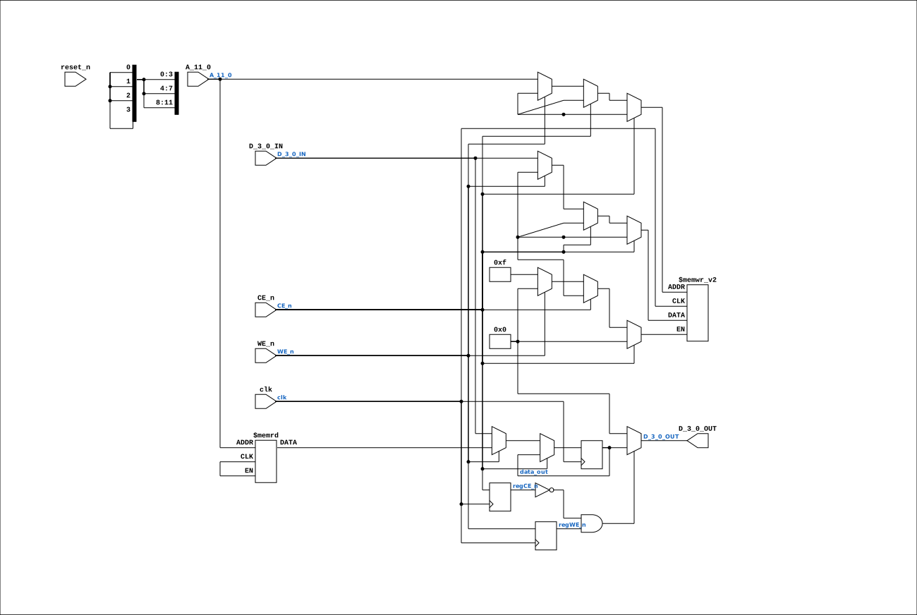
Drawn from the Verilog: the yosys netlist of the Simulation (Verilator) build, instance CORE.CPU_BOARD.CPU.CS.WCS.CHIP_16C. Sub-modules are boxes (click the picture to open it full size; there every sub-module box links to its page, and every wire shows its Verilog name).
Description
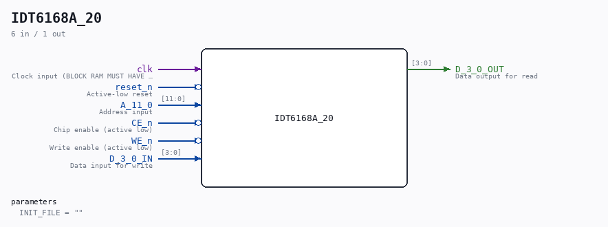
ND120 Shared IDT6168A 16K (4Kx4) Static RAM (using BLOCK RAM) Last reviewed: 29-JAN-2025 Ronny Hansen
Parameters
| Parameter | Default |
|---|---|
INIT_FILE |
"" |
Ports
| Direction | Width | Name | Description |
|---|---|---|---|
| input | 1 |
clk |
Clock input (BLOCK RAM MUST HAVE CLOCK) |
| input | 1 |
reset_n (active low) |
Active-low reset |
| input | [11:0] |
A_11_0 |
Address input |
| input | 1 |
CE_n (active low) |
Chip enable (active low) |
| input | 1 |
WE_n (active low) |
Write enable (active low) |
| input | [3:0] |
D_3_0_IN |
Data input for write |
| output | [3:0] |
D_3_0_OUT |
Data output for read |
Verilog source
Verilog/Shared/support/IDT6168A_20.v on GitHub.
Show the Verilog of IDT6168A_20 (245 lines)
/**************************************************************************
** ND120 Shared                                                          **
**                                                                       **
**  IDT6168A                                                             **
**  16K (4Kx4) Static RAM  (using BLOCK RAM)                             **
**                                                                       **
** Last reviewed: 29-JAN-2025                                             **
** Ronny Hansen                                                          **
***************************************************************************/


/*

The IDT6168 is a 16,384-bit high-speed static RAM organized as 4K x 4.
It is fabricated using IDT’s high-performance, high-reliability CMOS technology.
This state-of-the-art technology, combined with innovative circuit design techniques,
provides a cost-effective approach forhigh-speed memory applications.Access times as fast 15ns are available.

The circuit also offers areduced power standby mode.
When CS goes HIGH, the circuit willautomatically go to, and remain in, a standby mode as long as CS remainsHIGH.

This capability provides significant system-level power and coolingsavings.
The low-power (LA) version also offers a battery backup dataretention  capability  where  the  circuit  typically
consumes only 1μW operating off a 2V battery.

All inputs and outputs of the IDT6168 areTTL-compatible and operate from a single 5V supply.
The IDT6168 is packaged in either a space saving 20-pin, 300-milceramic or plastic DIP or a 20-pin LCC providing
high board-level packing densities.

Military grade product is manufactured in compliance with the latest revision of MIL-STD-883, Class B,
making it ideally suited tomilitary temperature applications demanding the highest level of performance and reliability.


High-speed (equal access and cycle time)
  –   Military: 25/45ns (max.)
  –   Industrial: 25ns (max.)
  –   Commercial: 15/20/25ns (max.)

Documentation: https://www.alldatasheet.com/datasheet-pdf/view/65830/IDT/IDT6168.html


NOTE!! The access time is not immediate, meaning it takes 15-20 nanoseconds after the address has changed for the data to become valid on the output.

*/
module IDT6168A_20 #(
    // Optional preload image (one 4-bit hex nibble per line, 4096 lines).
    // Empty string = no preload (default). Used to pre-fill the WCS so the
    // runtime microcode load can be skipped - see docs/skip-wcs-load.md.
    parameter INIT_FILE = ""
) (
    input wire clk,     // Clock input (BLOCK RAM MUST HAVE CLOCK)
    input wire reset_n, // Active-low reset

    input  wire [11:0] A_11_0,    // Address input
    input  wire        CE_n,      // Chip enable (active low)
    input  wire        WE_n,      // Write enable (active low)
    input  wire [ 3:0] D_3_0_IN,  // Data input for write
    output wire [ 3:0] D_3_0_OUT  // Data output for read
);

`ifdef QUARTUS_RAM_INFER

  // ---------------------------------------------------------------------
  // Quartus arm (01-SEP-2026): the SAME array and the SAME 1-clock
  // write-first behaviour as the reference below, only restructured into a
  // shape Quartus 17.0 will map onto M10K. PLAIN VERILOG on purpose.
  //
  // HISTORY - the arm this replaced. The first Quartus arm (31-AUG-2026,
  // deleted 01-SEP-2026 once this one had booted the board) was an explicit
  // altsyncram megafunction. It shipped with outdata_reg_a="CLOCK0", which
  // put a SECOND register on the output: altsyncram ALWAYS registers the
  // address in synchronous mode, so the WCS read took TWO clocks against
  // this model's ONE. Every microinstruction arrived a clock late on that
  // board alone, the microsequencer ran one step out of alignment with the
  // cycle controller, and a nested microsubroutine return popped the wrong
  // address (001015 instead of the 002027 MACL pushed) - the CPU looped
  // forever in the interrupt-register microcode. See
  // docs/mister-microcode-loop.md. Nothing simulates a megafunction, so no
  // simulation could ever have caught it; the equivalence check of the day
  // compared it against a hand-written stub that was wrong by the same
  // clock. That is why the arm below is plain Verilog and the megafunction
  // is gone: Shared/support/sim/run_quartus_ram_equiv.sh compiles and runs
  // BOTH this arm and the reference and proves them cycle-identical. An arm
  // that can be tested is worth more than an arm that is "obviously" right.
  //
  // What Quartus objects to in the reference arm (measured, build v46):
  //     Info (276007): ... uninferred due to asynchronous read logic
  // for all 32 WCS chips, then
  //     Error (276003): Cannot convert all sets of registers into RAM ...
  // because 32 x 4K x 4 bits of flip-flops does not fit any device.
  // Nothing reads the array outside the clocked block, so the read is not
  // actually asynchronous. What it cannot map is the OUTPUT REGISTER: in
  // the reference, data_out loads from the ARRAY on a read but from
  // D_3_0_IN on a write. A register fed from a non-memory source cannot be
  // the M10K's own output register, so the array read is left with nowhere
  // synchronous to land - and M10K has no asynchronous read port (the same
  // limit that forces the async cache RAMs onto MLAB).
  //
  // NOTE this is a reading of the evidence, not a rule quoted from Intel's
  // documentation. The build is the proof, and build v47 (01-SEP-2026)
  // delivered it: uninferred RAM 34 -> 1, all 32 WCS chips in M10K, and the
  // board boots to the OPCOM prompt on this arm.
  //
  // The fix: give the array read a register of its own that does nothing
  // but hold array data, and rebuild the write-first bypass outside it from
  // ordinary flip-flops.
  //
  // ramstyle "no_rw_check": a read and a write can hit the same address in
  // the same cycle. The bypass mux already supplies the new data there, so
  // whatever the M10K hands back on that cycle is discarded. Saying so
  // stops Quartus building bypass hardware we do not need.
  (* ramstyle = "no_rw_check, M10K" *)
  reg [3:0] idt_memory_array[0:4095];

  // Same optional preload as the reference arm. Quartus honours an
  // `initial $readmemh` as M10K bitstream init - unlike the old megafunction
  // arm, which needed a separately generated .mif per chip
  // (fpga/mister/tools/wcs_hex_to_mif.py, deleted together with it).
`ifdef SKIP_WCS_LOAD
  initial begin
    if (INIT_FILE != "") $readmemh(INIT_FILE, idt_memory_array);
  end
`endif

  reg [3:0] mem_q   = 4'h0;   // pure array read - THIS is the M10K output reg
  reg [3:0] byp_q   = 4'h0;   // write data, held one clock to match mem_q
  reg       byp_sel = 1'b0;   // the last enabled cycle was a write
  reg       regCE_n = 1'b1;
  reg       regWE_n = 1'b1;

  always @(posedge clk) begin
    regCE_n <= CE_n;
    regWE_n <= WE_n;
    if (!CE_n) begin
      // Read on EVERY enabled cycle, with nothing but the enable gating it.
      // On a write cycle the fetched value is thrown away by the mux below.
      mem_q <= idt_memory_array[A_11_0];

      if (!WE_n) idt_memory_array[A_11_0] <= D_3_0_IN;

      byp_q   <= D_3_0_IN;
      byp_sel <= ~WE_n;
    end
    // CE_n high: mem_q, byp_q and byp_sel all hold, so the output holds -
    // exactly as data_out holds in the reference arm.
  end

  // Write-first bypass, rebuilt outside the memory read register.
  wire [3:0] data_out = byp_sel ? byp_q : mem_q;

  // Same output mask as the reference arm.
  assign D_3_0_OUT = (!regCE_n && regWE_n) ? data_out : 4'b0000;

`else

  // Memory array - 4K x 4-bit. Marked for block RAM inference on FPGA targets.
  // This is the REFERENCE arm: Vivado (ram_style), Gowin (syn_ramstyle) plus
  // plus Verilator and iverilog, all take it and all infer block RAM from
  // it. Quartus does not - it takes the QUARTUS_RAM_INFER arm above instead.
  // (Keep "Verilator" off the START of a comment line: Verilator reads a
  // comment beginning with that word as a lint metacomment and dies with
  // "Unknown verilator comment", which broke every sim build 01-SEP-2026.)
  //
  // MEASURED 01-SEP-2026 (build v46), correcting an earlier guess of mine:
  // adding Quartus's own "ramstyle" spelling here does NOT make Quartus
  // infer the array. It still reports every instance as
  //   Info (276007): ... uninferred due to asynchronous read logic
  // and fails Analysis & Synthesis trying to build them from flip-flops.
  // The attribute spelling was never the reason inference failed; the
  // structure of the output register is (see the QUARTUS_RAM_INFER arm).
  // "ramstyle" is left in place because it is the correct spelling to state
  // for Quartus and costs nothing, not because it fixes anything.
  //
  // Quartus also warns Warning (10306) on syn_ramstyle="block_ram": it does
  // recognise Synplify's attribute NAME but not Gowin's VALUE for it. That
  // warning is harmless - Quartus never builds this arm.
  (* syn_ramstyle = "block_ram", ram_style = "block", ramstyle = "M10K" *)
  reg [3:0] idt_memory_array[0:4095];

  // Optional block-RAM preload (bitstream INIT on FPGA; $readmemh in sim).
  // Only active under SKIP_WCS_LOAD; preserves BRAM inference (Xilinx + Gowin).
`ifdef SKIP_WCS_LOAD
  initial begin
    if (INIT_FILE != "") $readmemh(INIT_FILE, idt_memory_array);
  end
`endif

  // -----------------------------------------------------------------------
  // Unified sim/FPGA model: posedge-clk write-first synchronous RAM.
  //
  // Both branches now use the SAME timing semantics — no `ifdef VERILATOR_SIM`
  // divergence. Read latency is 1 sysclk: address change at posedge clk N
  // produces the corresponding data at posedge clk N+1.
  //
  // Why 1 sysclk and not zero/combinational:
  //
  //   With zero-delay reads, the WCS feedback loop (WCS→CSBITS→SC5/SC6→
  //   regREP→regW→CSA→LUA→WCS) collapses entirely within one MCLK=0 idle
  //   period. The TVEC dispatch chain (o000017→o000016→o002001) resolves
  //   in delta time without intermediate MCLK pulses, and o000016 LDLC is
  //   skipped (R81 in CGA_DCD captures the wrong CSCOMM).
  //
  //   The 1-sysclk read delay forces each TVEC chain step to take its own
  //   MCLK cycle, matching how the original ASIC's WCS RAM access time
  //   (15-20ns) was a significant fraction of the original cycle period.
  //
  // Why posedge-only (not negedge writes / negedge reads):
  //
  //   The previous model had VERILATOR_SIM doing reads on posedge but
  //   writes on negedge, while the FPGA branch did BOTH on negedge — the
  //   half-sysclk shift created a sim/FPGA divergence. Unifying both to
  //   posedge eliminates the divergence and gives the same timing model
  //   in iverilog, Verilator, and the FPGA block RAM.
  //
  // Block RAM inference: Vivado and Gowin both recognise the
  // "always @(posedge clk) begin if (we) mem[a] <= d; out <= mem[a]; end"
  // pattern as a write-first BRAM template.
  // -----------------------------------------------------------------------
  reg [3:0] data_out  = 4'h0;
  reg       regCE_n   = 1'b1;
  reg       regWE_n   = 1'b1;

  always @(posedge clk) begin
    regCE_n <= CE_n;
    regWE_n <= WE_n;
    if (!CE_n) begin
      if (!WE_n) begin
        // Write happens at posedge clk N. Read of the SAME address at the
        // same edge returns the just-written value (write-first behavior).
        idt_memory_array[A_11_0] <= D_3_0_IN;
        data_out                 <= D_3_0_IN;
      end else begin
        // Pure read: capture memory[A] into data_out for the next cycle.
        data_out                 <= idt_memory_array[A_11_0];
      end
    end
  end

  // Output: tri-state-equivalent. Drives data_out only when the registered
  // CE_n is asserted AND the registered WE_n is high (read mode).
  assign D_3_0_OUT = (!regCE_n && regWE_n) ? data_out : 4'b0000;

`endif

endmodule