Am9150
Source: Verilog/Shared/support/Am9150.v
Where it sits (Simulation): ND120_TOP > ND120_CORE > ND3202D > CPU_15 > CPU_MMU_24 > CPU_MMU_CACHE_25 > Am9150
- instance path: CORE.CPU_BOARD.CPU.MMU.CACHE.CHIP_21F
Used in: CPU_MMU_CACHE_25 (Simulation, Nexys, MEGA65 R6, MEGA65 R3, QMTECH, Basys3, Cmod)
Contains: no other modules.
Module hierarchy - All modules
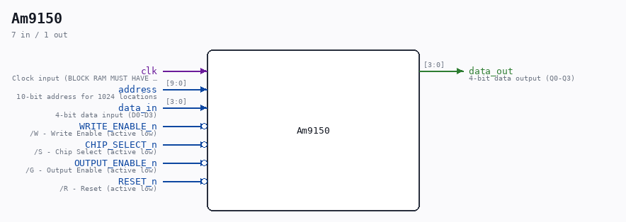
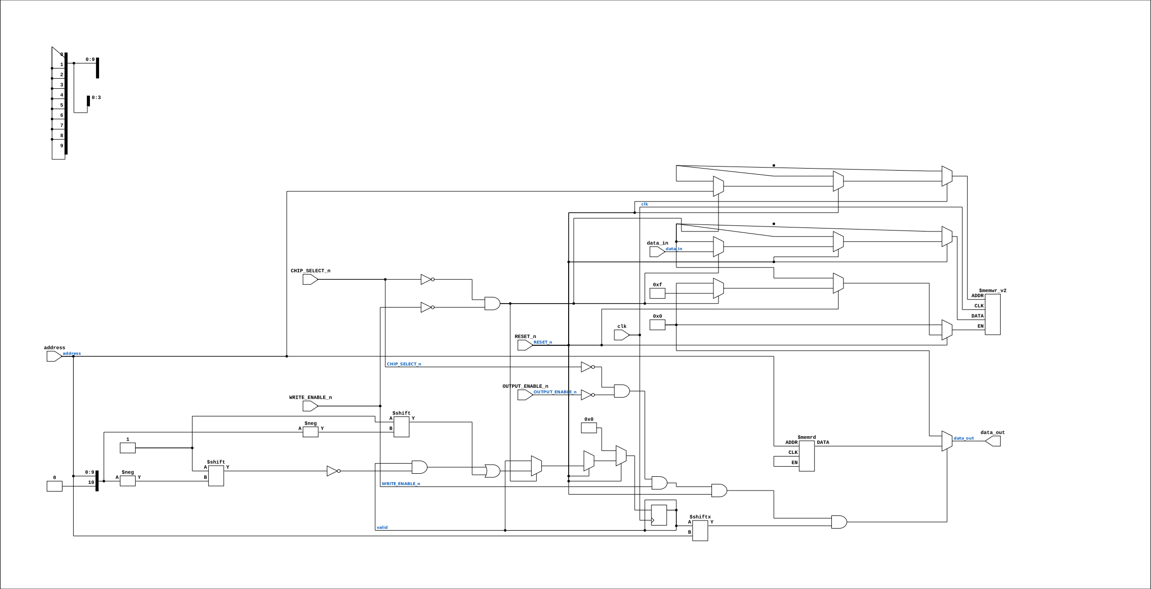
Schematic
Drawn from the Verilog: the yosys netlist of the Simulation (Verilator) build, instance CORE.CPU_BOARD.CPU.MMU.CACHE.CHIP_21F. Sub-modules are boxes (click the picture to open it full size; there every sub-module box links to its page, and every wire shows its Verilog name).
Description
ND120 Shared Component Am9150 Am9150 1024x4 High-Speed Static R/W RAM DISTINCTIVE CHARACTERISTICS • 1024 x 4 organization • High speed - 20 ns Max. access time • Separate data inputs and outputs • Memory reset function • High density SLIM 24-pin 300-MIL package • Three-state output buffers • Single + 5 V power supply ± 10% • Low-power version GENERAL DESCRIPTION The Am9150 is a high-performance, static, n-channel, read/write, random-access memory organized as 1024 x 4. It features single 5 V supply operation, TTL-compatible input and output levels, and separate input and output pins for improved system performance and ease of use. The Am9150 also incorporates a reset feature which will reset the entire contents of the memory to logical LOW in two cycle times by controlling /R (RESET) and /S (CS). The Am9150 has four control signals /R, /S, /W and /G. The /S input controls read, write and reset operations of the device and provides for easy selection of an individual device when the outputs are tied together. The /W (/WE) input controls the normal read and write operations, and the /G (/OE) controls the state of the outputs. http://www.sintran.com/library/libother/extern/AM9150.pdf Last reviewed: 2-FEB-2025 Ronny Hansen
Ports
| Direction | Width | Name | Description |
|---|---|---|---|
| input | 1 |
clk |
Clock input (BLOCK RAM MUST HAVE CLOCK) |
| input | [9:0] |
address |
10-bit address for 1024 locations |
| input | [3:0] |
data_in |
4-bit data input (D0-D3) |
| output | [3:0] |
data_out |
4-bit data output (Q0-Q3) |
| input | 1 |
WRITE_ENABLE_n (active low) |
/W - Write Enable (active low) |
| input | 1 |
CHIP_SELECT_n (active low) |
/S - Chip Select (active low) |
| input | 1 |
OUTPUT_ENABLE_n (active low) |
/G - Output Enable (active low) |
| input | 1 |
RESET_n (active low) |
/R - Reset (active low) |
Verilog source
Verilog/Shared/support/Am9150.v on GitHub.
Show the Verilog of Am9150 (113 lines)
/*******************************************************************************************************************************
** ND120 Shared                                                                                                               **
**                                                                                                                            **
** Component Am9150                                                                                                           **
**                                                                                                                            **
** Am9150 1024x4 High-Speed Static R/W RAM                                                                                    **
**                                                                                                                            **
**                                                                                                                            **
** DISTINCTIVE CHARACTERISTICS                                                                                                **
**  • 1024 x 4 organization                                                                                                   **
**  • High speed - 20 ns Max. access time                                                                                     **
**  • Separate data inputs and outputs                                                                                        **
**  • Memory reset function                                                                                                   **
**  • High density SLIM 24-pin 300-MIL package                                                                                **
**  • Three-state output buffers                                                                                              **
**  • Single + 5 V power supply ± 10%                                                                                         **
**  • Low-power version                                                                                                       **
**                                                                                                                            **
**  GENERAL DESCRIPTION                                                                                                       **
**                                                                                                                            **
**  The Am9150 is a high-performance, static, n-channel, read/write, random-access memory organized as 1024 x 4.              **
**  It features single 5 V supply operation, TTL-compatible input and output levels,                                          **
**  and separate input and output pins for improved system performance and ease of use.                                       **
**                                                                                                                            **
**  The Am9150 also incorporates a reset feature which will reset the entire contents of the memory to logical                **
**   LOW in two cycle times by controlling /R (RESET) and /S (CS).                                                            **
**                                                                                                                            **
**  The Am9150 has four control signals /R, /S, /W and /G.                                                                    **
**  The /S input controls read, write and reset operations of the device and provides for easy                                **
**  selection of an individual device when the outputs are tied together.                                                     **
**  The /W (/WE) input controls the normal read and write operations, and the /G (/OE)                                        **
**  controls the state of the outputs.                                                                                        **
**                                                                                                                            **
**  http://www.sintran.com/library/libother/extern/AM9150.pdf                                                                 **
**                                                                                                                            **
** Last reviewed: 2-FEB-2025                                                                                                  **
** Ronny Hansen                                                                                                               **
********************************************************************************************************************************/

module Am9150 (
    input  wire       clk,              // Clock input (BLOCK RAM MUST HAVE CLOCK)
    input  wire [9:0] address,          // 10-bit address for 1024 locations
    input  wire [3:0] data_in,          // 4-bit data input (D0-D3)
    output wire [3:0] data_out,         // 4-bit data output (Q0-Q3)
    input  wire       WRITE_ENABLE_n,   // /W - Write Enable (active low)
    input  wire       CHIP_SELECT_n,    // /S - Chip Select (active low)
    input  wire       OUTPUT_ENABLE_n,  // /G - Output Enable (active low)
    input  wire       RESET_n           // /R - Reset (active low)
);
  reg  [3:0] data4bit;

  /*******************************************************************************
   ** Memory array - distributed LUT RAM on every FPGA flow: the read below is  **
   ** asynchronous (the real chip is a 20 ns SRAM), which no block RAM can do.  **
   ** 1024x4 = 4 Kbit (~256 LUT4); one instance in the design (MMU cache        **
   ** CHIP_21F, the used/valid bits).                                            **
   *******************************************************************************/
  //! Vivado spells this `ram_style`, Quartus spells it `ramstyle`, and each
  //! ignores the other's. Stating only the Vivado one made Quartus fall back
  //! to flip-flops - see the long note in TMM2018D_25.v, where the same
  //! omission cost 65,536 registers and forced the MiSTer cache to be
  //! compiled out entirely.
  (* ram_style = "distributed", ramstyle = "MLAB" *)
  reg [3:0] am_memory_array[0:1023];

  /*******************************************************************************
   ** RESET (/R) - the real chip resets the ENTIRE memory to 0 "in two cycle   **
   ** times" (datasheet, controlling /R and /S).                                **
   **                                                                         **
   ** History, because this location has been wrong twice:                    **
   **  - the first model skipped the reset ("NO CAN DO WITH BLOCK RAM") and    **
   **    only gated data_out while /R was low, so CCLR was a no-op and stale  **
   **    pre-DMA lines kept hitting (24-AUG-2026, CPU_MMU_CACHE_DMA_tb.v);    **
   **  - the 24-AUG fix cleared the array with a 1024-step write sweep and    **
   **    DROPPED every external write while the sweep ran, saying that "only  **
   **    causes a spurious later miss". It did: CACHE-1X0-A00 test 2 issues a **
   **    cache clear and writes its test word within the next few hundred     **
   **    clocks, the tag and data RAMs took the write, this chip did not, and **
   **    the line stayed "not used" forever - "DATA is taken FROM MEMORY when **
   **    present in DATA CACHE", "NOT COPIED", "MIXED UP ADDRESSING" on the    **
   **    board and in Verilator alike (29-AUG-2026, runSim ND120_CACHE_WIN:   **
   **    sweep=1 at the write, used_mem=0 after it).                          **
   **                                                                         **
   ** Now: one VALID flip-flop per location. /R low clears all 1024 in ONE     **
   ** clock (the chip's two cycle times); a write sets its location's valid   **
   ** bit together with the data; a read returns 0 for a location that has   **
   ** not been written since the last reset. Nothing is ever dropped or       **
   ** swept. Power-up: the valid vector initialises to 0, so the X/random    **
   ** power-up contents of the array are never visible. Cost on the FPGA:    **
   ** 1024 flip-flops, on a board that has 126k.                              **
   *******************************************************************************/
  reg [1023:0] valid = {1024{1'b0}};

  // Read, write and reset operations
  always @(posedge clk)
  begin
    if (!RESET_n) begin
      valid <= {1024{1'b0}};             // /R: everything invalid at once
    end else if (!CHIP_SELECT_n && !WRITE_ENABLE_n) begin
      // Write operation: active when chip is selected and write enable is low
      am_memory_array[address] <= data_in;
      valid[address]           <= 1'b1;
    end

    data4bit <= valid[address] ? am_memory_array[address] : 4'b0000;   // registered copy for waveforms/probes
  end

  // Read operation: active when chip is selected and output enable is low
  // (and not writing, not in reset); a never-written location reads 0.
  assign data_out = (!CHIP_SELECT_n & !OUTPUT_ENABLE_n & WRITE_ENABLE_n & RESET_n & valid[address])
                    ? am_memory_array[address] : 4'b0;

endmodule