MEM_RAM_49_SDRAM
Source: Verilog/fpga/tang-nano-20k/sdram-bridge/MEM_RAM_49_SDRAM.v
Where it sits (Tang): ND120_TANG20K_TOP > ND120_CORE > ND3202D > MEM_43 > MEM_RAM_49_SDRAM
- instance path: CORE.CPU_BOARD.MEM.RAM
Used in: MEM_43 (Tang, MiSTer, MEGA65 R6, QMTECH)
Contains: sdram18
Module hierarchy - All modules
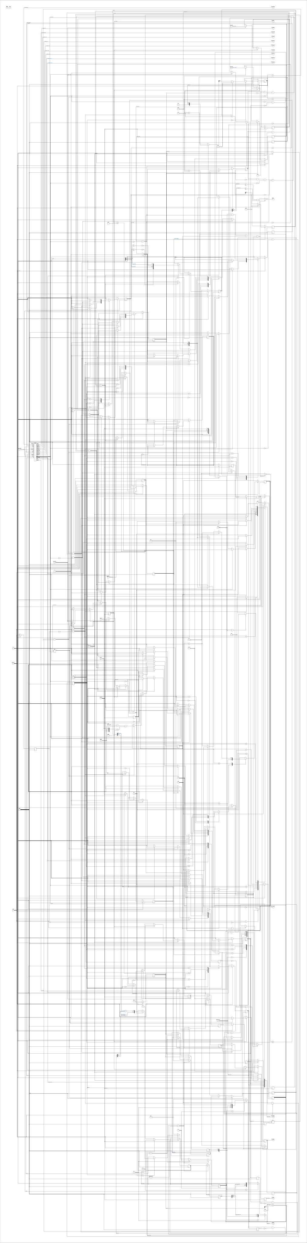
Schematic
Drawn from the Verilog: the yosys netlist of the Tang Nano 20K build, instance CORE.CPU_BOARD.MEM.RAM. Sub-modules are boxes (click the picture to open it full size; there every sub-module box links to its page, and every wire shows its Verilog name).
Description
ND120 CPU, MM&M MEM/RAM - SDRAM backend (Tang Nano 20K) Drop-in replacement for the sheet-49 RAM (MEM_RAM_49) that maps the ND-120 DRAM protocol onto the board's 8 MB embedded SDRAM through the 18-bit-word controller (sdram18.v). Protocol contract (measured, docs/nd120-dram-memory.md section 4; N = OSC cycle of the RAS rising edge, fast = 2x OSC, edge-aligned): N : row on AA_9_0, MWRITE50_n and BANKx valid N+1 : column on AA_9_0 N+2 : CAS rises, write data DD_17_0_IN valid N+4 : read data must be on DD_17_0_OUT (held while CAS high) N+5 : RAS falls, CAS tail one more cycle Next access no earlier than N+11. Capacity: 2M x 18-bit words = BANK0 + BANK2 (1M words each) = 4 MB. BANK1 is not populated: never written, reads as 0, so the ND-120's boot-time memory sizing simply detects two banks. (The board PAL decodes phys banks in the order BANK0,BANK2,BANK1 - so the CONTIGUOUS second 2 MB is BANK2, and BANK0+BANK2 is the real 4 MB; see line 373.) ND_SDRAM_PACK16 (docs/build-defines.md section 1, semantics pinned by docs/nd120-parity-analysis.md): only the 16 DATA bits are stored, two adjacent ND words per 32-bit SDRAM location, so BANK0+BANK2 (still the full 4 MB, boot sizing unchanged) fold into the LOWER half of the chip (location bit 20 = 0); the upper half is RESERVED for the nd_storage disk-image cache (nd-storage-design.md section 5.2). Parity is COMPUTED on the read path (DD[8]/DD[17] regenerated as odd parity, CORR_n always "correct") - licensed by the parity analysis: no self-test or runtime path reads stored parity. The CPU/storage split is parameterized at ND-row granularity (CPU_PART_ROWS) so a future build can trade CPU memory for cache. ND_STORAGE_PORT (requires ND_SDRAM_PACK16): adds the nd_storage device port of nd-storage-design.md section 5.2 - a start/busy/done mem port (stor_clk domain, toggle-CDC into clk2x) that reads/writes whole 32-bit locations at {1'b1, mem_addr[19:0]}, i.e. ONLY the upper-half storage region: the leading 1 is forced HERE, so device traffic physically cannot reach the CPU's half of the chip. Device ops are granted exactly like refresh - in the guaranteed-idle B_POST slot after each CPU access (>= 14 free fast cycles before the earliest next access under the N+11 rule; one op is 5 cycles), in B_TAIL (absent-row accesses leave the controller idle), and in B_IDLE behind the same idle_cnt watchdog guard - so CPU accesses always win and the measured protocol timing is untouched. Without the define the module is bit-identical to the plain pack16 build. Refresh is generated HERE (the board logic's refresh chain is inactive - see docs/nd120-dram-memory.md section 4): primarily in the guaranteed-idle slot right after each access, plus an idle watchdog when the CPU leaves memory alone. Last reviewed: 11-JUL-2026 Ronny Hansen
Parameters
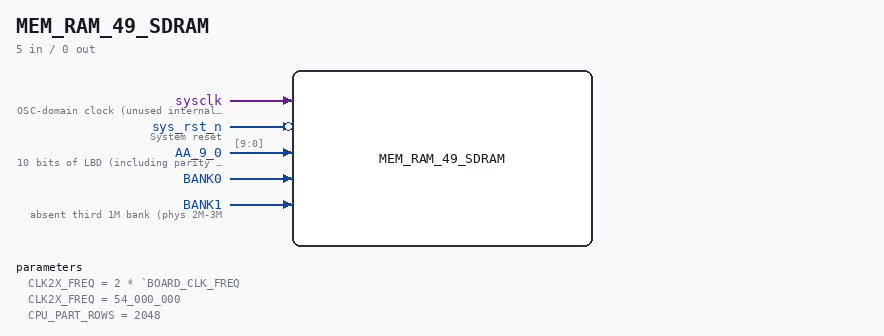
| Parameter | Default |
|---|---|
CLK2X_FREQ |
2 *BOARD_CLK_FREQ` |
CLK2X_FREQ |
54_000_000 |
CPU_PART_ROWS |
2048 |
Ports
| Direction | Width | Name | Description |
|---|---|---|---|
| input | 1 |
sysclk |
OSC-domain clock (unused internally; kept for symmetry) |
| input | 1 |
sys_rst_n (active low) |
System reset |
| input | [9:0] |
AA_9_0 |
10 bits of LBD (including parity in bit 10)- 10 bit input to MEM/RAM (from MEM_ADDR_44.AA_9_0) |
| input | 1 |
BANK0 |
|
| input | 1 |
BANK1 |
absent third 1M bank (phys 2M-3M |
Verilog source
Verilog/fpga/tang-nano-20k/sdram-bridge/MEM_RAM_49_SDRAM.v on GitHub.
Show the Verilog of MEM_RAM_49_SDRAM (645 lines)
/**************************************************************************
** ND120 CPU, MM&M **
** MEM/RAM - SDRAM backend (Tang Nano 20K) **
** Drop-in replacement for the sheet-49 RAM (MEM_RAM_49) that maps the **
** ND-120 DRAM protocol onto the board's 8 MB embedded SDRAM through **
** the 18-bit-word controller (sdram18.v). **
** **
** Protocol contract (measured, docs/nd120-dram-memory.md section 4; **
** N = OSC cycle of the RAS rising edge, fast = 2x OSC, edge-aligned): **
** N : row on AA_9_0, MWRITE50_n and BANKx valid **
** N+1 : column on AA_9_0 **
** N+2 : CAS rises, write data DD_17_0_IN valid **
** N+4 : read data must be on DD_17_0_OUT (held while CAS high) **
** N+5 : RAS falls, CAS tail one more cycle **
** Next access no earlier than N+11. **
** **
** Capacity: 2M x 18-bit words = BANK0 + BANK2 (1M words each) = 4 MB. **
** BANK1 is not populated: never written, reads as 0, so the ND-120's **
** boot-time memory sizing simply detects two banks. (The board PAL **
** decodes phys banks in the order BANK0,BANK2,BANK1 - so the CONTIGUOUS **
** second 2 MB is BANK2, and BANK0+BANK2 is the real 4 MB; see line 373.) **
** **
** ND_SDRAM_PACK16 (docs/build-defines.md section 1, semantics **
** pinned by docs/nd120-parity-analysis.md): only the 16 DATA bits are **
** stored, two adjacent ND words per 32-bit SDRAM location, so **
** BANK0+BANK2 (still the full 4 MB, boot sizing unchanged) fold into **
** the LOWER half of the chip (location bit 20 = 0); the upper half is **
** RESERVED for the nd_storage disk-image cache (nd-storage-design.md **
** section 5.2). Parity is COMPUTED on the read path (DD[8]/DD[17] **
** regenerated as odd parity, CORR_n always "correct") - licensed by the **
** parity analysis: no self-test or runtime path reads stored parity. **
** The CPU/storage split is parameterized at ND-row granularity **
** (CPU_PART_ROWS) so a future build can trade CPU memory for cache. **
** **
** ND_STORAGE_PORT (requires ND_SDRAM_PACK16): adds the nd_storage **
** device port of nd-storage-design.md section 5.2 - a start/busy/done **
** mem port (stor_clk domain, toggle-CDC into clk2x) that reads/writes **
** whole 32-bit locations at {1'b1, mem_addr[19:0]}, i.e. ONLY the **
** upper-half storage region: the leading 1 is forced HERE, so device **
** traffic physically cannot reach the CPU's half of the chip. Device **
** ops are granted exactly like refresh - in the guaranteed-idle B_POST **
** slot after each CPU access (>= 14 free fast cycles before the **
** earliest next access under the N+11 rule; one op is 5 cycles), in **
** B_TAIL (absent-row accesses leave the controller idle), and in **
** B_IDLE behind the same idle_cnt watchdog guard - so CPU accesses **
** always win and the measured protocol timing is untouched. Without **
** the define the module is bit-identical to the plain pack16 build. **
** **
** Refresh is generated HERE (the board logic's refresh chain is **
** inactive - see docs/nd120-dram-memory.md section 4): primarily in **
** the guaranteed-idle slot right after each access, plus an idle **
** watchdog when the CPU leaves memory alone. **
** **
** Last reviewed: 11-JUL-2026 **
** Ronny Hansen **
***************************************************************************/
module MEM_RAM_49_SDRAM #(
// Frequency of clk2x (= 2x OSC). MEM_43 instantiates this module without
// parameters, so the default must track the board clock: when the build
// provides BOARD_CLK_FREQ (tang20k_defines.v), derive 2x from it - the
// refresh interval and the controller's init counts depend on it.
`ifdef BOARD_CLK_FREQ
parameter CLK2X_FREQ = 2 * `BOARD_CLK_FREQ,
`else
parameter CLK2X_FREQ = 54_000_000,
`endif
// ND_SDRAM_PACK16 only: how many 1K-ND-word rows ({bank, row[9:0]} out of
// 2048) belong to the CPU. Default 2048 = full 4 MB main memory (both ND
// banks). Rows at/above this count report ABSENT (read 0, writes dropped),
// so boot-time sizing shrinks accordingly - e.g. 1024 = 2 MB CPU, freeing
// 6 MB of the chip for the storage cache. Keep it a multiple of 1024 so
// whole ND banks appear/disappear (the sizing probe works per bank).
parameter CPU_PART_ROWS = 2048
) (
// Input signals (sheet-49 interface, same as MEM_RAM_49)
input sysclk, // OSC-domain clock (unused internally; kept for symmetry)
input sys_rst_n, // System reset
input [9:0] AA_9_0, //! 10 bits of LBD (including parity in bit 10)- 10 bit input to MEM/RAM (from MEM_ADDR_44.AA_9_0)
input BANK0,
/* verilator lint_off UNUSEDSIGNAL */
input BANK1, // absent third 1M bank (phys 2M-3M); not populated here
/* verilator lint_on UNUSEDSIGNAL */
input BANK2, // 2nd populated 1M bank: PAL decodes phys 1M-2M here
input CAS,
input RAS,
input MWRITE50_n,
input [17:0] DD_17_0_IN,
output [17:0] DD_17_0_OUT,
output CORR_n,
// Fast clock domain (2x OSC from the same rPLL, edge-aligned)
input clk2x,
input clk2x_sdram, // 180 degrees from clk2x, for the SDRAM chip
// SDRAM device pins ("magic" names on Gowin EDA; pinned in the OSS cst)
output O_sdram_clk,
output O_sdram_cke,
output O_sdram_cs_n,
output O_sdram_cas_n,
output O_sdram_ras_n,
output O_sdram_wen_n,
inout [31:0] IO_sdram_dq,
output [10:0] O_sdram_addr,
output [ 1:0] O_sdram_ba,
output [ 3:0] O_sdram_dqm,
// Raw bridge state for the on-chip analyzer (see TRACE-CAPTURE-GUIDE.md)
output [ 7:0] DBG_BRIDGE,
//! ---- PAGE-WRITE WATCH (24-AUG-2026, zero-page campaign) ---------------
//! Run 15 measured that the page the CPU fetches zeros from is PPN 0o3770
//! = physical page 2040 = {bank_q=1 (BANK2), row_q=1016}, which is REAL
//! populated memory. So the disc data was never stored there. This bus
//! reports every access to the 8-page window rows 1016..1023 in BOTH
//! banks, AT THE BRIDGE - the last point before the SDRAM itself, so a
//! transfer that never arrives cannot be argued away.
//! word A: [15:14]=10 [13]=bank [12:3]=row [2:0]=data[15:13]
//! word B: [15:14]=11 [13:1]=data[12:0] [0]=0
//! read : [15:14]=01 [13]=bank [12:3]=row [2:0]=0
//! idle = 16'h0000
output [15:0] DBG_PGW
`ifdef ND_SDRAM_PACK16
`ifdef ND_STORAGE_PORT
// nd_storage device port (nd-storage-design.md section 5.2): 32-bit
// locations at {1'b1, mem_addr} = the upper-half storage region only
,
input wire stor_clk, // = clk_stor (nd_storage's memory side)
input wire stor_rst_n,
input wire mem_start, // 1-cycle pulse, only legal when mem_busy=0
input wire mem_we,
input wire [19:0] mem_addr, // 32-bit-location address inside the region
input wire [31:0] mem_wdata,
output reg [31:0] mem_rdata, // valid at mem_done, then held
output wire mem_busy,
output reg mem_done // 1-cycle pulse
`endif
`endif
);
/*******************************************************************************
** Write-data capture - OR-accumulation across the access **
** **
** Hardware evidence (Tang, 8-JUL-2026, four builds): the write data on **
** DD_17_0_IN appears only as a SUB-CYCLE PULSE somewhere inside the access **
** window - the AM29833A transceivers in MEM_DATA_46 drive it **
** combinationally, gated by PAL-generated OET_n/OER_n whose FF-mode phase **
** is narrow; every fixed sample point tried (2N+5 / 2N+9 / OSC N+2 / N+3) **
** read a dead or half-risen bus. The saving property: when NOT driving, **
** the transceiver outputs hard ZEROS (T_OUT = mode ? data : 0). So **
** OR-accumulate DD on every clk2x edge across the access: idle samples **
** contribute nothing, and with the pulse ~an OSC cycle wide, at least one **
** 74 ns-spaced sample lands inside it with all bits driven. **
*******************************************************************************/
reg [17:0] dd_acc;
// Second sampler on the falling clk2x edge: 37 ns effective granularity,
// in case the drive pulse is narrower than one clk2x period
reg [17:0] dd_acc_n;
reg ras_dn;
always @(negedge clk2x) begin
if (!sys_rst_n) begin
dd_acc_n <= 0;
ras_dn <= 0;
end else begin
ras_dn <= RAS;
if (RAS && !ras_dn) dd_acc_n <= DD_17_0_IN;
else if (RAS || CAS) dd_acc_n <= dd_acc_n | DD_17_0_IN;
end
end
/*******************************************************************************
** SDRAM controller (18-bit word variant, runs entirely on clk2x) **
*******************************************************************************/
reg s_rd, s_wr, s_refresh;
`ifdef ND_SDRAM_PACK16
reg [21:0] s_addr; // half-word address: [21]=0 pins the CPU to the low half
reg [15:0] s_din;
wire [15:0] s_dout;
`ifdef ND_STORAGE_PORT
// stor_clk-side request latches (stable from mem_start until mem_done, so
// safe to sample in clk2x once the synced start toggle arrives)
reg s_dev_busy;
reg s_dev_we_l;
reg [19:0] s_dev_addr_l;
reg [31:0] s_dev_wdata_l;
reg s_dev_start_tgl; // stor_clk -> clk2x request
reg s_dev_dn_s0, s_dev_dn_s1, s_dev_dn_d; // done toggle, synced back
// clk2x-side device engine
reg s_dev_st_s0, s_dev_st_s1, s_dev_st_d; // start toggle, synced in
reg s_dev_pend; // request waiting for a grant slot
reg s_dev_run; // op issued to the controller
reg s_dev_seen; // controller busy observed since issue
reg s_dev_done_tgl; // clk2x -> stor_clk completion
reg [31:0] s_dev_rdata; // dout32 captured at data_ready, held for stor_clk
reg s_acc32; // full-location command qualifier to sdram18
wire [31:0] s_dout32;
`endif
`else
reg [20:0] s_addr;
reg [17:0] s_din;
wire [17:0] s_dout;
`endif
wire s_data_ready, s_busy;
sdram18 #(
.FREQ(CLK2X_FREQ)
) u_sdram (
.clk(clk2x),
.clk_sdram(clk2x_sdram),
.resetn(sys_rst_n),
.rd(s_rd),
.wr(s_wr),
.refresh(s_refresh),
.addr(s_addr),
.din(s_din),
.dout(s_dout),
`ifdef ND_SDRAM_PACK16
`ifdef ND_STORAGE_PORT
.acc32(s_acc32),
.din32(s_dev_wdata_l),
.dout32(s_dout32),
`else
.acc32(1'b0),
.din32(32'b0),
.dout32(),
`endif
`endif
.data_ready(s_data_ready),
.busy(s_busy),
`ifdef ND_SDRAM_DQ16
// 16-bit module: only the low half of the 32-bit port pair is a pin;
// IO_sdram_dq[31:16] is left unconnected at the board top
.SDRAM_DQ(IO_sdram_dq[15:0]),
`else
.SDRAM_DQ(IO_sdram_dq),
`endif
.SDRAM_A(O_sdram_addr),
.SDRAM_BA(O_sdram_ba),
.SDRAM_nCS(O_sdram_cs_n),
.SDRAM_nWE(O_sdram_wen_n),
.SDRAM_nRAS(O_sdram_ras_n),
.SDRAM_nCAS(O_sdram_cas_n),
.SDRAM_CLK(O_sdram_clk),
.SDRAM_CKE(O_sdram_cke),
.SDRAM_DQM(O_sdram_dqm)
);
/*******************************************************************************
** Refresh timer: one auto-refresh per ND_SDRAM_REFRESH_US (default 15 us) **
** **
** 15 us suits the Tang's 2K-row die (4096 refreshes per 64 ms). A 16-bit **
** DE10-Nano module (ND_SDRAM_DQ16) has 8192 rows and needs one auto-refresh **
** every 7.8 us at most; the MiSTer build sets ND_SDRAM_REFRESH_US=7. Auto- **
** refresh walks the chip's OWN row counter, so this cadence covers the **
** whole die however many rows the CPU actually uses. **
*******************************************************************************/
`ifndef ND_SDRAM_REFRESH_US
`define ND_SDRAM_REFRESH_US 15
`endif
localparam REFRESH_INTERVAL = CLK2X_FREQ / 1_000_000 * `ND_SDRAM_REFRESH_US;
reg [10:0] ref_cnt;
reg refresh_needed;
always @(posedge clk2x) begin
if (!sys_rst_n) begin
ref_cnt <= 0;
refresh_needed <= 0;
end else begin
ref_cnt <= ref_cnt + 1;
if (ref_cnt >= REFRESH_INTERVAL[10:0]) refresh_needed <= 1;
if (s_refresh) begin
ref_cnt <= 0;
refresh_needed <= 0;
end
end
end
/*******************************************************************************
** Protocol bridge state machine (clk2x domain) **
** **
** RAS/CAS/AA/BANKx/MWRITE50_n are OSC-domain registered-PAL outputs; clk2x **
** is the same PLL at exactly 2x, so they change only on every other clk2x **
** edge and are sampled here as synchronous signals (fast edge 2N+1 sees the **
** value OSC edge N produced). **
*******************************************************************************/
localparam B_IDLE = 3'd0;
localparam B_COLWAIT = 3'd1; // fast edge 2N+2: AA is switching to the column
localparam B_COL = 3'd2; // fast edge 2N+3: column valid -> issue read
localparam B_WRDATA = 3'd3; // fast edge 2N+5: DD_IN valid -> issue write
localparam B_RDWAIT = 3'd4; // wait for data_ready, capture and hold
localparam B_POST = 3'd5; // op done: run a refresh if one is due
localparam B_TAIL = 3'd6; // unpopulated bank: just wait out the access
reg [2:0] bstate;
reg ras_d;
reg [9:0] row_q;
// ---- page-write watch (see the DBG_PGW port comment) ----------------------
// The window is rows 1016..1023 (row_q[9:3] == 7'd127) in both banks, so a
// transfer that lands a few pages off the target is visible as a near miss
// instead of looking like "no write at all".
localparam [6:0] PGW_ROW_HI = 7'd127;
reg [1:0] pgw_phase = 2'd0;
reg pgw_bank = 1'b0;
reg [9:0] pgw_row = 10'd0;
reg [15:0] pgw_data = 16'd0;
wire pgw_match = (row_q[9:3] == PGW_ROW_HI);
assign DBG_PGW = (pgw_phase == 2'd1) ? {2'b10, pgw_bank, pgw_row, pgw_data[15:13]}
: (pgw_phase == 2'd2) ? {2'b11, pgw_data[12:0], 1'b0}
: (pgw_phase == 2'd3) ? {2'b01, pgw_bank, pgw_row, 3'b000}
: 16'h0000;
// Rising-edge detect on the controller's own issue pulses, so the record is
// taken at the moment the access is handed to the SDRAM - not at the board
// interface, where a dropped transfer would still look present. s_din is
// already updated by the time s_wr's edge is seen one cycle later.
reg s_wr_d = 1'b0;
reg s_rd_d = 1'b0;
always @(posedge clk2x) begin
s_wr_d <= s_wr;
s_rd_d <= s_rd;
if (pgw_phase != 2'd0) pgw_phase <= (pgw_phase == 2'd1) ? 2'd2 : 2'd0;
if (s_wr && !s_wr_d && pgw_match) begin
pgw_bank <= bank_q;
pgw_row <= row_q;
pgw_data <= s_din[15:0];
pgw_phase <= 2'd1;
end else if (s_rd && !s_rd_d && pgw_match) begin
pgw_bank <= bank_q;
pgw_row <= row_q;
pgw_phase <= 2'd3;
end
end
reg wn_q; // 1 = read (MWRITE50_n high)
reg bsel_q; // access hits a populated bank (BANK0/BANK2)
reg bank_q; // 0 = BANK0, 1 = BANK2 (the 2nd populated 1M bank)
reg [2:0] wcnt_q; // write-data settle counter (capture late in the window)
reg [17:0] dd_hold;
reg have_data;
assign DBG_BRIDGE = {bstate[2:0], // [7:5] FSM state (B_IDLE..B_TAIL)
s_wr, // [4] write command issued
s_rd, // [3] read command issued
s_data_ready, // [2] controller returned read data
have_data, // [1] read data held for DD_OUT
s_busy}; // [0] controller busy
// Idle watchdog: if the CPU leaves memory alone, refresh anyway
reg [6:0] idle_cnt;
localparam IDLE_REFRESH_AFTER = 7'd64; // fast cycles (~1.2 us at 54 MHz)
always @(posedge clk2x) begin
if (!sys_rst_n) begin
bstate <= B_IDLE;
ras_d <= 0;
s_rd <= 0;
s_wr <= 0;
s_refresh <= 0;
s_addr <= 0;
s_din <= 0;
row_q <= 0;
wn_q <= 1;
bsel_q <= 0;
bank_q <= 0;
wcnt_q <= 0;
dd_hold <= 0;
have_data <= 0;
idle_cnt <= 0;
`ifdef ND_SDRAM_PACK16
`ifdef ND_STORAGE_PORT
s_dev_st_s0 <= 0;
s_dev_st_s1 <= 0;
s_dev_st_d <= 0;
s_dev_pend <= 0;
s_dev_run <= 0;
s_dev_seen <= 0;
s_dev_done_tgl <= 0;
s_dev_rdata <= 0;
s_acc32 <= 0;
`endif
`endif
end else begin
// command outputs are 1-cycle pulses
s_rd <= 0;
s_wr <= 0;
s_refresh <= 0;
ras_d <= RAS;
`ifdef ND_SDRAM_PACK16
`ifdef ND_STORAGE_PORT
// ---- storage device port, clk2x side ----
s_acc32 <= 0; // command qualifier: pulses with s_rd/s_wr on device grants
// request toggle from stor_clk: 2-flop sync + edge detect -> pending
s_dev_st_s0 <= s_dev_start_tgl;
s_dev_st_s1 <= s_dev_st_s0;
s_dev_st_d <= s_dev_st_s1;
if (s_dev_st_s1 != s_dev_st_d) s_dev_pend <= 1;
// completion tracking: after a grant, watch the controller go busy and
// idle again; reads capture the full location at data_ready
if (s_dev_run) begin
if (s_busy) s_dev_seen <= 1;
if (s_data_ready) s_dev_rdata <= s_dout32;
if (s_dev_seen && !s_busy) begin
s_dev_run <= 0;
s_dev_seen <= 0;
s_dev_done_tgl <= ~s_dev_done_tgl; // rdata already stable
end
end
`endif
`endif
// OR-accumulate the write data across the access (see comment above):
// reset at RAS rise, collect every clk2x edge while the access runs
if (RAS && !ras_d) dd_acc <= DD_17_0_IN;
else if (RAS || CAS) dd_acc <= dd_acc | DD_17_0_IN;
// have_data lifecycle: set when a read completes, cleared when the next
// access starts; the CAS term in read_active closes the output window.
case (bstate)
B_IDLE: begin
if (RAS && !ras_d) begin // fast edge 2N+1: RAS rise seen, AA = row
row_q <= AA_9_0;
wn_q <= MWRITE50_n;
`ifdef ND_SDRAM_PACK16
// partition check at row granularity: rows beyond the CPU's share
// behave exactly like an unpopulated bank (B_TAIL path)
// NOTE: the board decode PAL (PAL_44445B) wires the three 1M-word
// banks in physical-address order BANK0, BANK2, BANK1 - so the
// CONTIGUOUS second 2 MB (phys words 1M-2M) is decoded as BANK2,
// not BANK1. The two populated SDRAM regions must therefore be
// BANK0 + BANK2 (BANK1 = the absent third bank at 2M-3M).
bsel_q <= (BANK0 | BANK2) && ({BANK2, AA_9_0} < CPU_PART_ROWS[11:0]);
`else
bsel_q <= BANK0 | BANK2;
`endif
bank_q <= BANK2;
have_data <= 0;
idle_cnt <= 0;
bstate <= B_COLWAIT;
end else begin
// idle watchdog refresh (only when no access is starting)
idle_cnt <= (idle_cnt == IDLE_REFRESH_AFTER) ? idle_cnt : idle_cnt + 1;
if (refresh_needed && !s_busy && idle_cnt == IDLE_REFRESH_AFTER) s_refresh <= 1;
`ifdef ND_SDRAM_PACK16
`ifdef ND_STORAGE_PORT
// device grant, behind the same long-idle guard as the watchdog
// refresh (refresh keeps priority; !s_refresh blocks the cycle a
// refresh pulse is still being presented to the controller)
else if (s_dev_pend && !s_dev_run && !s_busy && !s_refresh
&& idle_cnt == IDLE_REFRESH_AFTER) begin
s_addr <= {1'b1, s_dev_addr_l, 1'b0}; // storage half ONLY
s_acc32 <= 1;
if (s_dev_we_l) s_wr <= 1;
else s_rd <= 1;
s_dev_pend <= 0;
s_dev_run <= 1;
end
`endif
`endif
end
end
B_COLWAIT: bstate <= B_COL; // 2N+2: skip the AA row->column switch edge
B_COL: begin // 2N+3: AA carries the column
if (!bsel_q) begin
bstate <= B_TAIL; // BANK1 / no bank: not populated, do nothing
end else if (!s_busy) begin
`ifdef ND_SDRAM_PACK16
// ND word address as a HALF-WORD index into the low half of the
// chip: adjacent ND words share one 32-bit location ([0] = half)
s_addr <= {1'b0, bank_q, row_q, AA_9_0};
`else
s_addr <= {bank_q, row_q, AA_9_0}; // {bank, row[9:0], col[9:0]} = 21 bits
`endif
if (wn_q) begin
s_rd <= 1; // read: issue now -> data_ready by fast 2N+8 = OSC N+4
bstate <= B_RDWAIT;
end else begin
wcnt_q <= 0; // write: DD_IN settles DURING the both-low window
bstate <= B_WRDATA;
end
end
// if s_busy (watchdog refresh collided with this access) hold here;
// the refresh frees the controller within 5 fast cycles
end
B_WRDATA: begin
// Wait until the accumulated data has covered the whole possible
// drive window (through OSC N+4 = fast 2N+8), then issue with it
wcnt_q <= wcnt_q + 1'b1;
if (wcnt_q >= 3'd5 && !s_busy) begin
`ifdef ND_SDRAM_PACK16
// store the 16 DATA bits only; DD[8]/DD[17] (parity) are dropped
// and recomputed on read (docs/nd120-parity-analysis.md section 6)
s_din <= {dd_acc[16:9] | dd_acc_n[16:9], dd_acc[7:0] | dd_acc_n[7:0]};
`else
s_din <= dd_acc | dd_acc_n;
`endif
s_wr <= 1;
bstate <= B_POST;
end else if (wcnt_q >= 3'd5) begin
wcnt_q <= wcnt_q; // controller busy (colliding refresh): hold
end
end
B_RDWAIT:
if (s_data_ready) begin
`ifdef ND_SDRAM_PACK16
// regenerate ODD parity (AM29833A convention: PAR = ~^byte) so the
// downstream checkers and CORR_n always see a correct word
dd_hold <= {~(^s_dout[15:8]), s_dout[15:8], ~(^s_dout[7:0]), s_dout[7:0]};
`else
dd_hold <= s_dout;
`endif
have_data <= 1;
bstate <= B_POST;
end
B_POST:
if (!s_busy && !s_rd && !s_wr) begin
// guaranteed-idle slot: earliest next access is N+11 (22 fast cycles
// after RAS rise), a refresh takes 5 - always safe here
if (refresh_needed) s_refresh <= 1;
`ifdef ND_SDRAM_PACK16
`ifdef ND_STORAGE_PORT
// device grant in the same guaranteed-idle slot, refresh first: a
// 5-cycle device op issued here is long done before the earliest
// next access reaches B_COL (fast 2N+25)
else if (s_dev_pend && !s_dev_run && !s_refresh) begin
s_addr <= {1'b1, s_dev_addr_l, 1'b0}; // storage half ONLY
s_acc32 <= 1;
if (s_dev_we_l) s_wr <= 1;
else s_rd <= 1;
s_dev_pend <= 0;
s_dev_run <= 1;
end
`endif
`endif
bstate <= B_IDLE;
end
B_TAIL: begin
// absent bank/row: the controller is idle for this whole access, so
// it is a free refresh slot - without this, a run of absent-row
// accesses (each resetting the idle watchdog, none reaching the
// B_POST slot) starves refresh past its 15 us cadence
if (refresh_needed && !s_busy) s_refresh <= 1;
`ifdef ND_SDRAM_PACK16
`ifdef ND_STORAGE_PORT
// device grant in the absent-row free slot, refresh first: the op
// ends at latest 6 cycles after RAS fall, the next access is >= 12
else if (s_dev_pend && !s_dev_run && !s_busy && !s_refresh) begin
s_addr <= {1'b1, s_dev_addr_l, 1'b0}; // storage half ONLY
s_acc32 <= 1;
if (s_dev_we_l) s_wr <= 1;
else s_rd <= 1;
s_dev_pend <= 0;
s_dev_run <= 1;
end
`endif
`endif
if (!RAS) bstate <= B_IDLE;
end
default: bstate <= B_IDLE;
endcase
end
end
/*******************************************************************************
** Sheet-49 outputs: same gating as the SIP1M9 chips (drive 0 / parity 1 **
** when not selected or not reading, so downstream OR-combining still works) **
*******************************************************************************/
wire read_active = CAS & wn_q & bsel_q & have_data;
assign DD_17_0_OUT = read_active ? dd_hold : 18'b0;
// Two virtual SIP1M9 parity outputs (low chip = DD[8:0], high chip = DD[17:9]),
// remaining four (unpopulated banks) contribute constant 1 - same formula as
// SIP1M9's PRD_n, same AND-combination as MEM_RAM_49's CORR_n.
assign CORR_n = read_active ? ((^dd_hold[8:0]) & (^dd_hold[17:9])) : 1'b1;
`ifdef ND_SDRAM_PACK16
`ifdef ND_STORAGE_PORT
/*******************************************************************************
** Storage device port, stor_clk side (nd-storage-design.md section 5.2) **
** **
** start/we/addr/wdata are latched at the mem_start pulse and held stable **
** for the whole op, so the clk2x side samples them as quasi-static data **
** behind the 2-flop start-toggle sync. Completion comes back as a done **
** toggle; s_dev_rdata was captured at data_ready, several clk2x cycles **
** before the toggle flip, so it is stable when sampled here. **
*******************************************************************************/
assign mem_busy = s_dev_busy;
always @(posedge stor_clk) begin
if (!stor_rst_n) begin
s_dev_busy <= 0;
s_dev_we_l <= 0;
s_dev_addr_l <= 0;
s_dev_wdata_l <= 0;
s_dev_start_tgl <= 0;
s_dev_dn_s0 <= 0;
s_dev_dn_s1 <= 0;
s_dev_dn_d <= 0;
mem_rdata <= 0;
mem_done <= 0;
end else begin
mem_done <= 0;
s_dev_dn_s0 <= s_dev_done_tgl;
s_dev_dn_s1 <= s_dev_dn_s0;
s_dev_dn_d <= s_dev_dn_s1;
if (!s_dev_busy) begin
if (mem_start) begin
s_dev_we_l <= mem_we;
s_dev_addr_l <= mem_addr;
s_dev_wdata_l <= mem_wdata;
s_dev_busy <= 1;
s_dev_start_tgl <= ~s_dev_start_tgl;
end
end else if (s_dev_dn_s1 != s_dev_dn_d) begin
mem_rdata <= s_dev_rdata;
mem_done <= 1;
s_dev_busy <= 0;
end
end
end
`endif
`endif
endmodule