sdram18
Source: Verilog/fpga/tang-nano-20k/sdram-bridge/sdram18.v
Where it sits (Tang): ND120_TANG20K_TOP > ND120_CORE > ND3202D > MEM_43 > MEM_RAM_49_SDRAM > sdram18
- instance path: CORE.CPU_BOARD.MEM.RAM.u_sdram
Used in: MEM_RAM_49_SDRAM (Tang, MiSTer, MEGA65 R6, QMTECH)
Contains: no other modules.
Module hierarchy - All modules
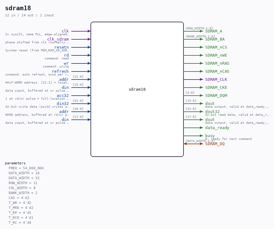
Schematic
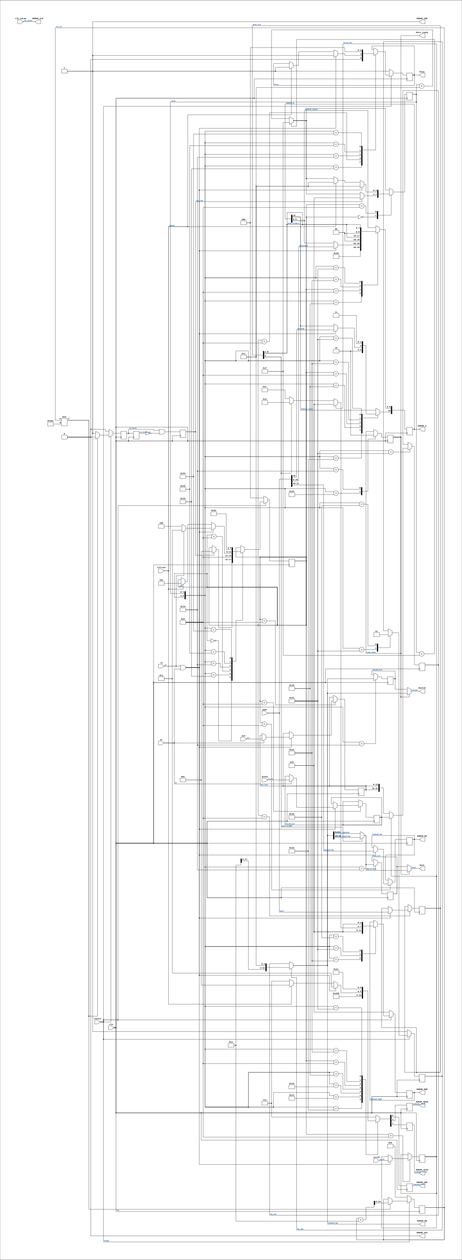
Drawn from the Verilog: the yosys netlist of the Tang Nano 20K build, instance CORE.CPU_BOARD.MEM.RAM.u_sdram. Sub-modules are boxes (click the picture to open it full size; there every sub-module box links to its page, and every wire shows its Verilog name).
Parameters
| Parameter | Default |
|---|---|
FREQ |
54_000_000 |
DATA_WIDTH |
16 |
DATA_WIDTH |
32 |
ROW_WIDTH |
11 |
COL_WIDTH |
8 |
BANK_WIDTH |
2 |
CAS |
4'd2 |
T_WR |
4'd2 |
T_MRD |
4'd2 |
T_RP |
4'd1 |
T_RCD |
4'd1 |
T_RC |
4'd4 |
Ports
| Direction | Width | Name | Description |
|---|---|---|---|
| inout | [DATA_WIDTH-1:0] |
SDRAM_DQ |
|
| output | [ROW_WIDTH-1:0] |
SDRAM_A |
|
| output | [BANK_WIDTH-1:0] |
SDRAM_BA |
|
| output | 1 |
SDRAM_nCS |
|
| output | 1 |
SDRAM_nWE |
|
| output | 1 |
SDRAM_nRAS |
|
| output | 1 |
SDRAM_nCAS |
|
| output | 1 |
SDRAM_CLK |
|
| output | 1 |
SDRAM_CKE |
|
| output | [3:0] |
SDRAM_DQM |
|
| input | 1 |
clk |
2x sysclk, same PLL, edge-aligned (from MEM_43.clk2x) |
| input | 1 |
clk_sdram |
phase shifted from clk (normally 180-degrees) |
| input | 1 |
resetn |
System reset (from MEM_RAM_49_SDRAM.sys_rst_n) |
| input | 1 |
rd |
command: read |
| input | 1 |
wr |
command: write |
| input | 1 |
refresh |
command: auto refresh, once per ~15 us |
| input | [21:0] |
addr |
HALF-WORD address: [21:1] = location, [0] = half |
| input | [15:0] |
din |
data input, buffered at wr pulse time |
| output | [15:0] |
dout |
data output, valid at data_ready, then held |
| input | 1 |
acc32 |
1 at rd/wr pulse = full-location (32-bit) op |
| input | [31:0] |
din32 |
32-bit write data (acc32 writes only) |
| output | [31:0] |
dout32 |
32-bit read data, valid at data_ready, held |
| input | [20:0] |
addr |
WORD address, buffered at rd/wr pulse time |
| input | [17:0] |
din |
data input, buffered at wr pulse time |
| output | [17:0] |
dout |
data output, valid at data_ready, then held |
| output | 1 |
data_ready |
|
| output | 1 |
busy |
0: ready for next command |
Verilog source
Verilog/fpga/tang-nano-20k/sdram-bridge/sdram18.v on GitHub.
Show the Verilog of sdram18 (339 lines)
// 18-bit-word SDRAM controller for Tang Nano 20K - ND-120 main memory variant
//
// Adapted from nand2mario's byte-based controller (sdram-test/src/sdram.v,
// Apache-2.0, see sdram-test/src/LICENSE.nand2mario). Differences:
//   - one 18-bit ND-120 word (16 data + 2 parity) per 32-bit SDRAM word,
//     upper 14 DQ bits unused
//   - addr is a 21-bit WORD address (2M words = the whole 8 MB part),
//     no byte offset / DQM lane selection: writes drive all four lanes
//   - everything else (timing parameters, state machine, refresh, init)
//     is unchanged
//
// ND_SDRAM_PACK16 (docs/build-defines.md section 1, semantics pinned by
// docs/nd120-parity-analysis.md): store 16 DATA bits only, TWO ND words per
// 32-bit SDRAM location. addr becomes a 22-bit HALF-WORD address
// ([21:1] = location, [0] = half), din/dout become 16 bits. A 16-bit write
// stays a SINGLE access: the DQM byte lanes mask the other half (write DQM
// latency is 0 cycles), so there is no read-modify-write and the state
// machine timing is untouched. After the write burst the DQM lanes are
// restored to 0 (read DQM latency is 2 cycles - a stale mask would blank
// the next read's data window on silicon). Reads fetch the full 32-bit
// location and mux the addressed half onto dout.
//
// Full-location access (pack16 only, for the nd_storage device port of
// MEM_RAM_49_SDRAM - nd-storage-design.md section 5.2): pulsing rd/wr with
// acc32=1 moves the WHOLE 32-bit location addressed by addr[21:1]
// (addr[0] is ignored): writes drive all four DQM lanes from din32, reads
// return the location on dout32. Same 5-cycle state machine, no timing
// change; with acc32 tied 0 the controller behaves bit-identically to the
// plain pack16 build.
//
// ND_SDRAM_DQ16 (MiSTer / DE10-Nano, 01-SEP-2026; requires ND_SDRAM_PACK16):
// the SDRAM module on that board is 16 bits wide (SDRAM_DQ[15:0], two DQM
// pins, A[12:0]). One ND word per 16-bit location, so the pack16 "two words
// per 32-bit location" folding disappears: addr[20:0] IS the location
// ({ba[1:0], row[10:0], col[7:0]}, addr[21] unused and 0), both byte lanes
// are always enabled, and the acc32/din32/dout32 full-location port is
// meaningless (dout32 returns the 16-bit word zero-extended). The client
// interface (16-bit din/dout, 22-bit addr, 5-cycle ops, 4-cycle read
// latency) is otherwise identical, so MEM_RAM_49_SDRAM needs no change
// beyond leaving the upper 16 DQ and upper 2 DQM bits unconnected at the
// board top. 2M locations = 4 MB, the same BANK0+BANK2 the Tang has. Any
// 16-bit module with at least 2048 rows x 256 columns x 4 banks holds it;
// refresh is the caller's job (MEM_RAM_49_SDRAM, ND_SDRAM_REFRESH_US).
//
// Under default settings (max 66.7Mhz):
// - Data read latency is 4 cycles, read/write take 5 cycles, no overlap.
// - All ops use auto-precharge; caller must pulse `refresh` once per ~15 us.
// - clk_sdram must be 180 degrees from clk (PLL clkoutp).

module sdram18
#(
    parameter         FREQ = 54_000_000,

`ifdef ND_SDRAM_DQ16
    parameter         DATA_WIDTH = 16,
`else
    parameter         DATA_WIDTH = 32,
`endif
    parameter         ROW_WIDTH = 11,  // 2K rows
    parameter         COL_WIDTH = 8,   // 256 words per row
    parameter         BANK_WIDTH = 2,  // 4 banks

    // Time delays for 66.7Mhz max clock (min clock cycle 15ns)
    parameter [3:0]   CAS  = 4'd2,
    parameter [3:0]   T_WR = 4'd2,
    parameter [3:0]   T_MRD= 4'd2,
    parameter [3:0]   T_RP = 4'd1,
    parameter [3:0]   T_RCD= 4'd1,
    parameter [3:0]   T_RC = 4'd4
)
(
    // SDRAM side interface
    inout [DATA_WIDTH-1:0]      SDRAM_DQ,
    output reg [ROW_WIDTH-1:0]  SDRAM_A,
    output reg [BANK_WIDTH-1:0] SDRAM_BA,
    output            SDRAM_nCS,
    output reg        SDRAM_nWE,
    output reg        SDRAM_nRAS,
    output reg        SDRAM_nCAS,
    output            SDRAM_CLK,
    output            SDRAM_CKE,
    output reg  [3:0] SDRAM_DQM,

    // Logic side interface
    input             clk,          //! 2x sysclk, same PLL, edge-aligned (from MEM_43.clk2x)
    input             clk_sdram,    // phase shifted from clk (normally 180-degrees)
    input             resetn,       //! System reset (from MEM_RAM_49_SDRAM.sys_rst_n)
    input             rd,           // command: read
    input             wr,           // command: write
    input             refresh,      // command: auto refresh, once per ~15 us
`ifdef ND_SDRAM_PACK16
    input      [21:0] addr,         // HALF-WORD address: [21:1] = location, [0] = half
    input      [15:0] din,          // data input, buffered at wr pulse time
    output     [15:0] dout,         // data output, valid at data_ready, then held
    input             acc32,        // 1 at rd/wr pulse = full-location (32-bit) op
    input      [31:0] din32,        // 32-bit write data (acc32 writes only)
    output     [31:0] dout32,       // 32-bit read data, valid at data_ready, held
`else
    input      [20:0] addr,         // WORD address, buffered at rd/wr pulse time
    input      [17:0] din,          // data input, buffered at wr pulse time
    output     [17:0] dout,         // data output, valid at data_ready, then held
`endif
    output reg        data_ready,
    output reg        busy          // 0: ready for next command
);

// Tri-state DQ input/output
reg dq_oen;         // 0 means output
reg [DATA_WIDTH-1:0] dq_out;
assign SDRAM_DQ = dq_oen ? {DATA_WIDTH{1'bz}} : dq_out;
wire [DATA_WIDTH-1:0] dq_in = SDRAM_DQ;

`ifdef ND_SDRAM_PACK16
reg [15:0] dout_buf;
wire [15:0] dq_in_half;
assign dout = data_ready ? dq_in_half : dout_buf;
reg [31:0] dout32_buf;
`ifdef ND_SDRAM_DQ16
wire [31:0] dq_in32 = {16'b0, dq_in};   // no full-location port on a 16-bit part
`else
wire [31:0] dq_in32 = dq_in;
`endif
assign dout32 = data_ready ? dq_in32 : dout32_buf;
`else
reg [17:0] dout_buf;
assign dout = data_ready ? dq_in[17:0] : dout_buf;
`endif
assign SDRAM_CLK = clk_sdram;
assign SDRAM_CKE = 1'b1;
assign SDRAM_nCS = 1'b0;

reg [2:0] state;
localparam INIT = 3'd0;
localparam CONFIG = 3'd1;
localparam IDLE = 3'd2;
localparam READ = 3'd3;
localparam WRITE = 3'd4;
localparam REFRESH = 3'd5;

// RAS# CAS# WE#
localparam CMD_SetModeReg=3'b000;
localparam CMD_AutoRefresh=3'b001;
localparam CMD_PreCharge=3'b010;
localparam CMD_BankActivate=3'b011;
localparam CMD_Write=3'b100;
localparam CMD_Read=3'b101;
localparam CMD_NOP=3'b111;

localparam [2:0] BURST_LEN = 3'b0;      // burst length 1
localparam BURST_MODE = 1'b0;           // sequential
localparam [10:0] MODE_REG = {4'b0, CAS[2:0], BURST_MODE, BURST_LEN};

reg cfg_now;            // pulse for configuration
reg [3:0] cycle;
`ifdef ND_SDRAM_PACK16
reg [15:0] din_buf;
reg [21:0] addr_buf;    // {ba[1:0], row[10:0], col[7:0], half}
`ifdef ND_SDRAM_DQ16
assign dq_in_half = dq_in[15:0];        // one word per location: no half select
`else
assign dq_in_half = addr_buf[0] ? dq_in[31:16] : dq_in[15:0];
`endif
reg        acc32_buf;   // full-location op, latched with addr_buf
reg [31:0] din32_buf;
`else
reg [17:0] din_buf;
reg [20:0] addr_buf;    // {ba[1:0], row[10:0], col[7:0]}
`endif

//
// SDRAM state machine
//
always @(posedge clk) begin
    cycle <= cycle == 4'd15 ? 4'd15 : cycle + 4'd1;
    // defaults
    {SDRAM_nRAS, SDRAM_nCAS, SDRAM_nWE} <= CMD_NOP;
    casex ({state, cycle})
        // wait 200 us on power-on
        {INIT, 4'bxxxx} : if (cfg_now) begin
            state <= CONFIG;
            cycle <= 0;
        end

        // configuration sequence
        {CONFIG, 4'd0} : begin
            // precharge all
            {SDRAM_nRAS, SDRAM_nCAS, SDRAM_nWE} <= CMD_PreCharge;
            SDRAM_A[10] <= 1'b1;
        end
        {CONFIG, T_RP} : begin
            {SDRAM_nRAS, SDRAM_nCAS, SDRAM_nWE} <= CMD_AutoRefresh;
        end
        {CONFIG, T_RP+T_RC} : begin
            {SDRAM_nRAS, SDRAM_nCAS, SDRAM_nWE} <= CMD_AutoRefresh;
        end
        {CONFIG, T_RP+T_RC+T_RC} : begin
            {SDRAM_nRAS, SDRAM_nCAS, SDRAM_nWE} <= CMD_SetModeReg;
            SDRAM_A[10:0] <= MODE_REG;
        end
        {CONFIG, T_RP+T_RC+T_RC+T_MRD} : begin
            state <= IDLE;
            busy <= 1'b0;
        end

        // read/write/refresh
        {IDLE, 4'bxxxx}: if (rd | wr) begin
            // bank activate; word address split: {ba, row, col}
            {SDRAM_nRAS, SDRAM_nCAS, SDRAM_nWE} <= CMD_BankActivate;
`ifdef ND_SDRAM_DQ16
            SDRAM_BA <= addr[20:19];                // 16-bit part: addr[20:0] is the location
            SDRAM_A  <= addr[18:8];                 // 11-bit row address
`elsif ND_SDRAM_PACK16
            SDRAM_BA <= addr[21:20];
            SDRAM_A  <= addr[19:9];                 // 11-bit row address
`else
            SDRAM_BA <= addr[20:19];
            SDRAM_A  <= addr[18:8];                 // 11-bit row address
`endif
            state <= rd ? READ : WRITE;
            addr_buf <= addr;
            if (wr) din_buf <= din;
`ifdef ND_SDRAM_PACK16
            acc32_buf <= acc32;
            if (wr) din32_buf <= din32;
`endif
            cycle <= 4'd1;
            busy <= 1'b1;
        end else if (refresh) begin
            {SDRAM_nRAS, SDRAM_nCAS, SDRAM_nWE} <= CMD_AutoRefresh;
            state <= REFRESH;
            cycle <= 4'd1;
            busy <= 1'b1;
        end

        // read sequence (data at cycle T_RCD+CAS+1 relative to activate)
        {READ, T_RCD}: begin
            {SDRAM_nRAS, SDRAM_nCAS, SDRAM_nWE} <= CMD_Read;
            SDRAM_A[10] <= 1'b1;        // auto precharge
`ifdef ND_SDRAM_DQ16
            SDRAM_A[9:0] <= {2'b0, addr_buf[COL_WIDTH-1:0]};  // column
`elsif ND_SDRAM_PACK16
            SDRAM_A[9:0] <= {2'b0, addr_buf[COL_WIDTH:1]};  // column (location)
`else
            SDRAM_A[9:0] <= {2'b0, addr_buf[COL_WIDTH-1:0]};  // column
`endif
            SDRAM_DQM <= 4'b0;
        end
        {READ, T_RCD+CAS}: begin
            data_ready <= 1'b1;
        end
        {READ, T_RCD+CAS+4'd1}: begin
            data_ready <= 1'b0;
`ifdef ND_SDRAM_PACK16
            dout_buf <= dq_in_half;
            dout32_buf <= dq_in32;
`else
            dout_buf <= dq_in[17:0];
`endif
            busy <= 0;
            state <= IDLE;
        end

        // write sequence
        {WRITE, T_RCD}: begin
            {SDRAM_nRAS, SDRAM_nCAS, SDRAM_nWE} <= CMD_Write;
            SDRAM_A[10] <= 1'b1;        // auto precharge
`ifdef ND_SDRAM_DQ16
            SDRAM_A[9:0] <= {2'b0, addr_buf[COL_WIDTH-1:0]};  // column
            SDRAM_DQM <= 4'b0000;       // both byte lanes: one word per location
            dq_out <= din_buf;
`elsif ND_SDRAM_PACK16
            SDRAM_A[9:0] <= {2'b0, addr_buf[COL_WIDTH:1]};  // column (location)
            // lane-masked single-access write: mask (1) the half NOT addressed;
            // full-location (acc32) writes drive all four lanes from din32
            SDRAM_DQM <= acc32_buf ? 4'b0000 : (addr_buf[0] ? 4'b0011 : 4'b1100);
            dq_out <= acc32_buf ? din32_buf
                                : {din_buf, din_buf};  // masked lanes ignore their copy
`else
            SDRAM_A[9:0] <= {2'b0, addr_buf[COL_WIDTH-1:0]};  // column
            SDRAM_DQM <= 4'b0000;       // write all lanes (18-bit word in 32)
            dq_out <= {14'b0, din_buf};
`endif
            dq_oen <= 1'b0;
        end
        {WRITE, T_RCD+4'd1}: begin
            dq_oen <= 1'b1;
`ifdef ND_SDRAM_PACK16
            // restore read mask NOW: read DQM latency is 2 cycles, so the mask
            // must be low well before the next read's data window
            SDRAM_DQM <= 4'b0;
`endif
        end
        {WRITE, T_RCD+T_WR+T_RP}: begin
            busy <= 0;
            state <= IDLE;
        end

        // refresh sequence
        {REFRESH, T_RC}: begin
            state <= IDLE;
            busy <= 0;
        end
    endcase

    if (~resetn) begin
        busy <= 1'b1;
        dq_oen <= 1'b1;
        SDRAM_DQM <= 4'b0;
        state <= INIT;
    end
end

//
// Generate cfg_now pulse after initialization delay (normally 200us)
//
reg  [14:0]   rst_cnt;
reg rst_done, rst_done_p1, cfg_busy;

always @(posedge clk) begin
    rst_done_p1 <= rst_done;
    cfg_now     <= rst_done & ~rst_done_p1;

    if (rst_cnt != FREQ / 1000 * 200 / 1000) begin      // count to 200 us
        rst_cnt  <= rst_cnt[14:0] + 1;
        rst_done <= 1'b0;
        cfg_busy <= 1'b1;
    end else begin
        rst_done <= 1'b1;
        cfg_busy <= 1'b0;
    end

    if (~resetn) begin
        rst_cnt  <= 15'd0;
        rst_done <= 1'b0;
        cfg_busy <= 1'b1;
    end
end

endmodule