DECODE_DGA_POW
Source: Verilog/DECODE-GateArray/DGA/circuit/DECODE_DGA_POW.v
Where it sits (Simulation): ND120_TOP > ND120_CORE > ND3202D > IO_37 > IO_DCD_38 > DECODE_DGA > DECODE_DGA_POW
- instance path: CORE.CPU_BOARD.IO.DCD.DGA.POW
Used in: DECODE_DGA (all tops)
Contains: F091, F103, F571, F595 x5, F714 x3, J_K_FLIPFLOP x3
Module hierarchy - All modules
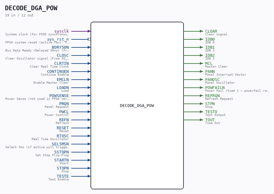
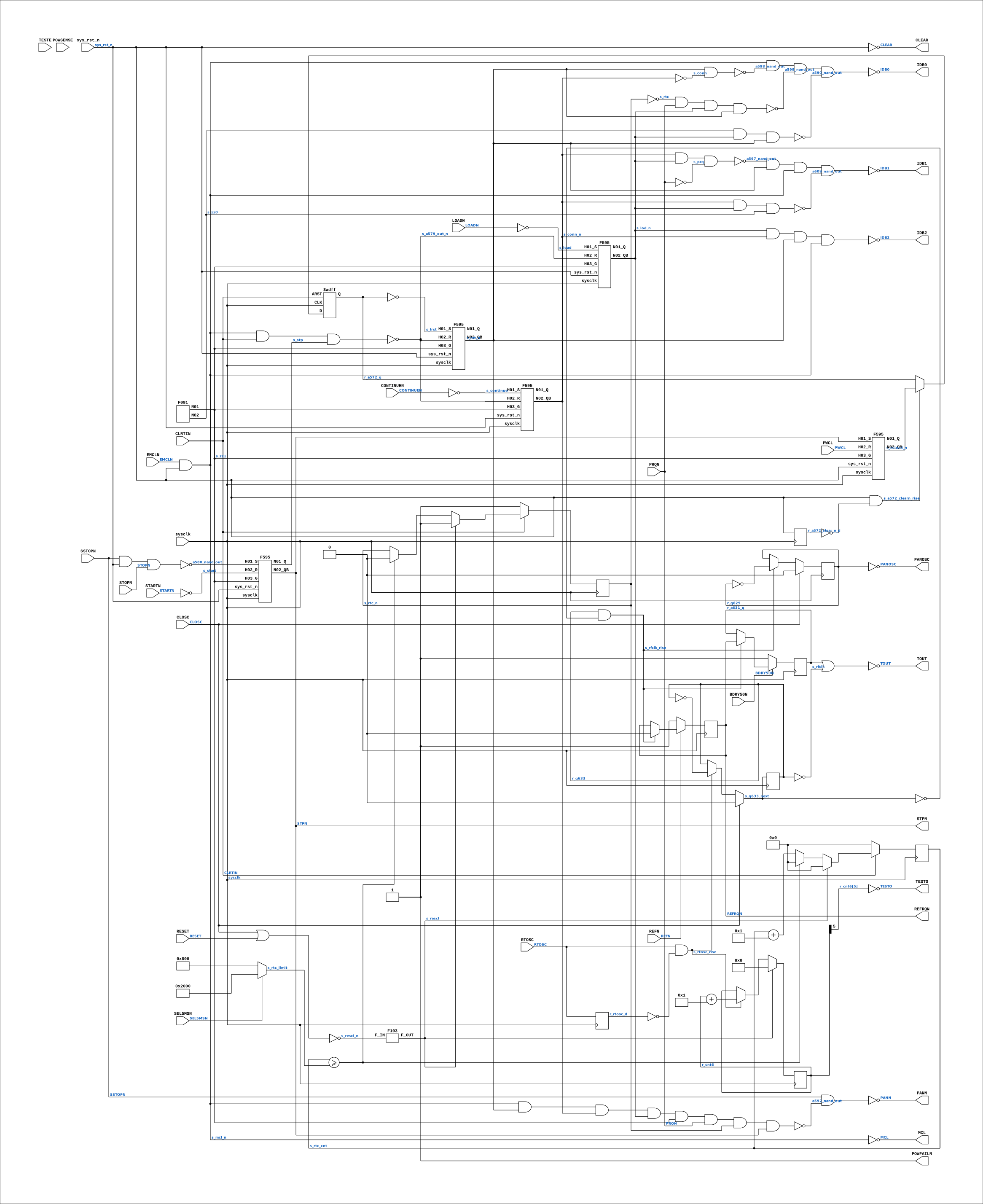
Schematic
Drawn from the Verilog: the yosys netlist of the Simulation (Verilator) build, instance CORE.CPU_BOARD.IO.DCD.DGA.POW. Sub-modules are boxes (click the picture to open it full size; there every sub-module box links to its page, and every wire shows its Verilog name).
Description
ND120 DGA DECODE/DGA/POW Page 8 DECODE - DECODE_DGA_POW- Sheet 1 of 3 Page 9 DECODE - DECODE_DGA_POW- Sheet 2 of 3 Page 10 DECODE - DECODE_DGA_POW- Sheet 3 of 3 Last reviewed: 2-FEB-2025 Ronny Hansen FPGA changes: - sys_rst_n added: forces all F595 RS latches to idle (Q=0,Qn=1) during FPGA reset, preventing boot lockup from uninitialized state - Powerfail logic removed (A596,A602,A593,A594,A591,A605,A600,A601) Not needed on FPGA — sys_rst_n replaces powerfail-driven reset - A569 (CLEAR latch) replaced by assign s_clear_n = sys_rst_n This pulses CLEAR during the FPGA reset window (replaces powerfail → CLEAR chain). Releases when sys_rst_n goes high at boot. - RTC counter replaced with synchronous sysclk counter (A577 was the original D_FF; A623/A619/A624/A616/A618/A617/A625 chain was unreliable in FPGA fabric due to cascaded data-signal clocks). - VERILATOR_SIM: short RTC count (8192/2048 cycles) for fast sim. Matches original TESTE=1 F714-chain effective period (~8K cycles). Fast enough for simulation, slow enough for instruction verify. FPGA: real 20ms/5ms count at 100 MHz.
Ports
| Direction | Width | Name | Description |
|---|---|---|---|
| input | 1 |
sysclk |
System clock (for F595 synchronous RS latch on FPGA) |
| input | 1 |
sys_rst_n (active low) |
FPGA system reset (active-low): forces latches to idle, pulses CLEAR |
| input | 1 |
BDRY50N |
Bus Data Ready (Delayed 50ns) (from BIF_5.BDRY50_n) |
| input | 1 |
CLOSC |
Clear Oscillator signal (From IO_DCD_38) - High briefly at power-on then 0 |
| input | 1 |
CLRTIN |
Clear Real Time Clock |
| input | 1 |
CONTINUEN |
Continue Enable |
| input | 1 |
EMCLN |
Enable Master Clear |
| input | 1 |
LOADN |
Load |
| input | 1 |
POWSENSE |
Power Sense (not used in FPGA version — powerfail removed) |
| input | 1 |
PRQN |
Panel Request |
| input | 1 |
PWCL |
Power Control |
| input | 1 |
REFN |
Refresh |
| input | 1 |
RESET |
Reset |
| input | 1 |
RTOSC |
Real Time Oscillator |
| input | 1 |
SEL5MSN |
Select 5ms (if active will trigger RTC after 5ms, not 20ms) |
| input | 1 |
SSTOPN |
Set Stop Flip-Flop |
| input | 1 |
STARTN |
Start |
| input | 1 |
STOPN |
Stop |
| input | 1 |
TESTE |
Test Enable |
| output | 1 |
CLEAR |
Clear signal |
| output | 1 |
IDB0 |
IDB 0 |
| output | 1 |
IDB1 |
IDB 1 |
| output | 1 |
IDB2 |
IDB 2 |
| output | 1 |
MCL |
Master Clear |
| output | 1 |
PANN |
Panel Interrupt Vector |
| output | 1 |
PANOSC |
Panel Oscillator |
| output | 1 |
POWFAILN |
Power Fail (tied 1 — powerfail removed in FPGA version) |
| output | 1 |
REFRQN |
Refresh Request |
| output | 1 |
STPN |
Stop |
| output | 1 |
TESTO |
Test Output |
| output | 1 |
TOUT |
Time Out |
Verilog source
Verilog/DECODE-GateArray/DGA/circuit/DECODE_DGA_POW.v on GitHub.
Show the Verilog of DECODE_DGA_POW (662 lines)
/**************************************************************************
** ND120 DGA                                                             **
** DECODE/DGA/POW                                                        **
**                                                                       **
**  Page 8 DECODE - DECODE_DGA_POW- Sheet 1 of 3                         **
**  Page 9 DECODE - DECODE_DGA_POW- Sheet 2 of 3                         **
**  Page 10 DECODE - DECODE_DGA_POW- Sheet 3 of 3                        **
**                                                                       **
** Last reviewed: 2-FEB-2025                                             **
** Ronny Hansen                                                          **
**                                                                       **
** FPGA changes:                                                         **
**  - sys_rst_n added: forces all F595 RS latches to idle (Q=0,Qn=1)    **
**    during FPGA reset, preventing boot lockup from uninitialized state **
**  - Powerfail logic removed (A596,A602,A593,A594,A591,A605,A600,A601) **
**    Not needed on FPGA — sys_rst_n replaces powerfail-driven reset     **
**  - A569 (CLEAR latch) replaced by assign s_clear_n = sys_rst_n       **
**    This pulses CLEAR during the FPGA reset window (replaces powerfail **
**    → CLEAR chain). Releases when sys_rst_n goes high at boot.        **
**  - RTC counter replaced with synchronous sysclk counter (A577 was    **
**    the original D_FF; A623/A619/A624/A616/A618/A617/A625 chain was   **
**    unreliable in FPGA fabric due to cascaded data-signal clocks).     **
**  - VERILATOR_SIM: short RTC count (8192/2048 cycles) for fast sim.   **
**    Matches original TESTE=1 F714-chain effective period (~8K cycles). **
**    Fast enough for simulation, slow enough for instruction verify.    **
**    FPGA: real 20ms/5ms count at 100 MHz.                             **
***************************************************************************/

module DECODE_DGA_POW (
    // System
    input sysclk,      // System clock (for F595 synchronous RS latch on FPGA)
    input sys_rst_n,   // FPGA system reset (active-low): forces latches to idle, pulses CLEAR
    // Inputs
    input BDRY50N,    //! Bus Data Ready (Delayed 50ns) (from BIF_5.BDRY50_n)
    input CLOSC,        //! Clear Oscillator signal (From IO_DCD_38) - High briefly at power-on then 0
    input CLRTIN,       //! Clear Real Time Clock
    input CONTINUEN,    //! Continue Enable
    input EMCLN,        //! Enable Master Clear
    input LOADN,        //! Load
    input POWSENSE,     //! Power Sense (not used in FPGA version — powerfail removed)
    input PRQN,         //! Panel Request
    input PWCL,         //! Power Control
    input REFN,         //! Refresh
    input RESET,        //! Reset
    input RTOSC,        //! Real Time Oscillator
    input SEL5MSN,  //! Select 5ms (if active will trigger RTC after 5ms, not 20ms)
    input SSTOPN,   //! Set Stop Flip-Flop
    input STARTN,   //! Start
    input STOPN,    //! Stop
    input TESTE,    //! Test Enable

    // Outputs
    output CLEAR,     //! Clear signal
    output IDB0,      //! IDB 0
    output IDB1,      //! IDB 1
    output IDB2,      //! IDB 2
    output MCL,       //! Master Clear
    output PANN,      //! Panel Interrupt Vector
    output PANOSC,    //! Panel Oscillator
    output POWFAILN,  //! Power Fail (tied 1 — powerfail removed in FPGA version)
    output REFRQN,    //! Refresh Request
    output STPN,      //! Stop
    output TESTO,     //! Test Output
    output TOUT       //! Time Out
);

  /*******************************************************************************
   ** The wires are defined here                                                 **
   *******************************************************************************/
  wire a580_nand_out;
  wire a590_nand_out;
  wire a592_nand_out;
  wire a597_nand_out;
  wire a598_nand_out;
  wire a599_nand_out;
  wire a609_nand_out;
  wire s_a579_out_n;
  wire s_a616_q;
  wire s_a617_q_n;
  wire s_a618_q_n;
  wire s_a618_q;
  wire s_a620_y;
  wire s_a621_q_n;
  wire s_a622_q_n;
  wire s_a623_q_n;
  wire s_a624_q_n;
  wire s_a626_q_n;
  wire s_a627_q_n;
  wire s_a631_q;
  wire s_a632_q_n;
  wire s_a634_q_n;
  wire s_bdry50_n;
  wire s_clear_n;
  wire s_clear;
  wire s_closc;
  wire s_clrti_n;
  wire s_clrti;
  wire s_conn_n;
  wire s_conn;
  wire s_continue_n;
  wire s_continue;
  wire s_emcl_n;
  wire s_esload_n;
  wire s_gnd;
  wire s_idb0;
  wire s_idb1;
  wire s_idb2;
  wire s_load_n;
  wire s_load;
  wire s_lod_n;
  wire s_lrst;
  wire s_mcl_n;
  wire s_mcl;
  wire s_pan_n;
  wire s_panosc;
  wire s_powfail_n;
  wire s_powfail;
  wire s_prq_n;
  wire s_prq;
  wire s_pwcl_n;
  wire s_pwcl;
  wire s_ref_n;
  wire s_refrq_n;
  wire s_rescl_n;
  wire s_rescl;
  wire s_reset;
  wire s_rfclk;
  wire s_rst_n;
  wire s_rtc_n;
  wire s_rtc;
  wire s_rtosc;
  wire s_sel5ms_n;
  wire s_sstop_n;
  wire s_start_n;
  wire s_start;
  wire s_stop_n;
  wire s_stp_n;
  wire s_stp;
  wire s_test_enable;
  wire s_testo;
  wire s_tout;
  wire s_vcc;
  wire s_zz0;
  wire s_zz1;

  /*******************************************************************************
   ** Here all input connections are defined                                     **
   *******************************************************************************/
  assign s_bdry50_n = BDRY50N;
  assign s_closc = CLOSC;
  assign s_clrti_n = CLRTIN;
  assign s_continue_n = CONTINUEN;
  assign s_emcl_n = EMCLN;
  assign s_load_n = LOADN;
  // POWSENSE not used in FPGA version (powerfail removed)
  assign s_prq_n = PRQN;
  assign s_pwcl = PWCL;
  assign s_ref_n = REFN;
  assign s_reset = RESET;
  assign s_rtosc = RTOSC;
  assign s_sel5ms_n = SEL5MSN;
  assign s_sstop_n = SSTOPN;
  assign s_start_n = STARTN;
  assign s_stop_n = STOPN;
  assign s_test_enable = TESTE;

  /*******************************************************************************
   ** Here all output connections are defined                                    **
   *******************************************************************************/
  assign CLEAR = s_clear;
  assign IDB0 = s_idb0;
  assign IDB1 = s_idb1;
  assign IDB2 = s_idb2;
  assign MCL = s_mcl;
  assign PANN = s_pan_n;
  assign PANOSC = s_panosc;
  assign POWFAILN = s_powfail_n;  // Tied 1 — powerfail removed
  assign REFRQN = s_refrq_n;
  assign STPN = s_stp_n;
  assign TESTO = s_testo;
  assign TOUT = s_tout;

  /*******************************************************************************
   ** Here all in-lined components are defined                                   **
   *******************************************************************************/

  // Ground and power
  assign s_gnd = 1'b0;
  assign s_vcc = 1'b1;

  // Powerfail removed: tie powerfail signals to safe/inactive state
  assign s_powfail   = 1'b0;
  assign s_powfail_n = 1'b1;

  // NOT Gate's
  assign s_clear = ~s_clear_n;
  assign s_clrti = ~s_clrti_n;
  assign s_conn = ~s_conn_n;
  assign s_continue = ~s_continue_n;
  assign s_load = ~s_load_n;
  assign s_mcl_n = ~s_mcl;
  assign s_prq = ~s_prq_n;
  assign s_pwcl_n = ~s_pwcl;
  assign s_rtc = ~s_rtc_n;
  assign s_start = ~s_start_n;

  /*******************************************************************************
   ** Here all normal components are defined                                     **
   *******************************************************************************/

  // A597 NAND_GATE_3_INPUTS
  assign a597_nand_out = ~(s_conn_n & s_lod_n & s_prq);

  //A609 NAND_GATE_3_INPUTS
  assign a609_nand_out = ~(s_conn_n & s_lod_n & s_zz0);

  // A598 NAND_GATE
  assign a598_nand_out = ~(s_rst_n & s_conn);

  // A599 NAND_GATE_4_INPUTS
  assign a599_nand_out = ~(s_rtc & s_prq_n & s_lod_n & s_rst_n);

  // A590 NAND_GATE_3_INPUTS
  assign a590_nand_out = ~(s_zz0 & s_lod_n & s_rst_n);

  // A580 NAND_GATE_3_INPUTS
  assign a580_nand_out = ~(s_sstop_n & s_clear_n & s_stop_n);

  // A606 NAND_GATE_4_INPUTS
  assign s_idb2 = ~(s_lod_n & s_conn_n & s_rst_n & s_mcl_n);

  //A592 NAND_GATE_8_INPUTS
`ifdef TANG_NO_RTC_PAN
  // DIAGNOSTIC (masked-level-10 root cause): drop the RTC's contribution to the
  // PAN (panel/timing) request so the free-running RTC raises NO interrupt. If
  // the phantom macro-interrupt / PIL->10 wedge vanishes with this, the held RTC
  // PAN was the source (conkick already exonerated).
  assign a592_nand_out = ~(s_mcl_n & s_rst_n & s_conn_n & s_lod_n & s_zz1 & s_prq_n & 1'b1 & s_stp_n);
`else
  assign a592_nand_out = ~(s_mcl_n & s_rst_n & s_conn_n & s_lod_n & s_zz1 & s_prq_n & s_rtc_n & s_stp_n);
`endif

  // A603 NAND_GATE_4_INPUTS
  assign s_idb1 = ~(a597_nand_out & s_rst_n & s_mcl_n & a609_nand_out);

  // A604 NAND_GATE_4_INPUTS
  assign s_idb0 = ~(s_mcl_n & a598_nand_out & a599_nand_out & a590_nand_out);

  // A595 NAND_GATE
  assign s_pan_n = ~(s_sstop_n & a592_nand_out);

  //A573 NAND_GATE
  assign s_mcl = ~(s_emcl_n & s_clear_n);

  // A636 NOR GATE
  assign s_tout = ~(s_a631_q | s_rfclk);

  // A635 NOR_GATE
  assign s_rescl_n = ~(s_closc | s_reset);

  // A579 NAND_GATE_3_INPUTS
  assign s_a579_out_n = ~(s_mcl_n & s_clrti_n & s_stp);

  // A569 CLEAR latch replaced: pulse CLEAR during FPGA reset window (sys_rst_n=0),
  // then release. This replaces the original powerfail -> CLEAR chain.
  // CLEAR_n=0 (active) during reset -> MCL fires, initialising all modules.
  // CLEAR_n=1 after reset -> MCL inactive, boot proceeds normally.
  assign s_clear_n = sys_rst_n;

  J_K_FLIPFLOP #(
      .InvertClockEnable(0)
  ) A616 (
      .clock(s_a624_q_n),
      .j(s_a618_q_n),
      .k(s_vcc),
      .preset(s_gnd),
      .q(s_a616_q),
      .qBar(),
      .reset(s_rescl),
      .tick(1'b1)
  );

  J_K_FLIPFLOP #(
      .InvertClockEnable(0)
  ) A618 (
      .clock(s_a624_q_n),
      .j(s_a616_q),
      .k(s_vcc),
      .preset(s_gnd),
      .q(s_a618_q),
      .qBar(s_a618_q_n),
      .reset(s_rescl),
      .tick(1'b1)
  );

  J_K_FLIPFLOP #(
      .InvertClockEnable(0)
  ) A617 (
      .clock(s_a624_q_n),
      .j(s_a618_q),
      .k(s_a618_q),
      .preset(s_gnd),
      .q(),
      .qBar(s_a617_q_n),
      .reset(s_rescl),
      .tick(1'b1)
  );

`ifdef FPGA_FF_MODE
  // P4 (docs/plan-fix-unconstrained-clocks.md): s_clear_n (= sys_rst_n on
  // FPGA) was A572's clock pin - the last register/reset-net clock root
  // (Gowin auto-created a bogus 100MHz "sys_rst_n" base clock for it and
  // could not analyze any path touching it). Capture s_esload_n on a
  // sysclk-detected clear_n rise instead; the async CLRTI preset is kept.
  reg r_a572_clear_n_d = 1'b0;
  always @(posedge sysclk) r_a572_clear_n_d <= s_clear_n;
  wire s_a572_clearn_rise = s_clear_n & ~r_a572_clear_n_d;

  reg r_a572_q = 1'b0;  // q starts 0 -> s_lrst (qBar) starts 1, as the original
  always @(posedge sysclk or posedge s_clrti) begin
    if (s_clrti) r_a572_q <= 1'b1;
    else if (s_a572_clearn_rise) r_a572_q <= s_esload_n;
  end
  assign s_lrst = ~r_a572_q;
`else
  D_FLIPFLOP #(.ACTIVE_ASYNC(1),
      .InvertClockEnable(0)
  ) A572 (
      .clock(s_clear_n),
      .d(s_esload_n),
      .preset(s_clrti),
      .q(),
      .qBar(s_lrst),
      .reset(s_zz0),  //negated zz1
      .tick(1'b1)
  );
`endif

  // A577: RTC (Real Time Clock) — synchronous sysclk counter replaces the
  // F714/JK ripple chain (A623->A619->A624->A616/A618/A617 chain) which uses
  // cascaded data-signal clocks unreliable in FPGA fabric.
  //
  // Simulation: short count (256 cycles) so boot completes quickly.
  // FPGA: real-time 20ms/5ms count at 100MHz.
  // BOARD_CLK_FREQ: actual frequency of sysclk in Hz. The Basys3 build defines
  // it (vivado_build.tcl: 16666667 for the 16.67 MHz clk_cpu); default matches
  // the SC2661_UART.v fallback so both timers share one clock assumption.
`ifndef BOARD_CLK_FREQ
  `define BOARD_CLK_FREQ 100_000_000
`endif

`ifdef RTC_REAL_PERIOD
  // Force the REAL board-clock period even in a Verilator build - used to
  // reproduce FPGA real-time behavior (OPCOM output pacing) in simulation.
  localparam RTC_20MS = (`BOARD_CLK_FREQ / 50) - 1;    // 20 ms
  localparam RTC_5MS  = (`BOARD_CLK_FREQ / 200) - 1;   // 5 ms
`elsif VERILATOR_SIM
  // Original TESTE=1 F714 chain: RTOSC(period=256cyc) -> /2(A624) -> /8(A616/A618/A617) -> /2(A577) ~ 8192 sysclk per interrupt
  // 256 was too fast (32x) - instruction verify programs couldn't execute enough instructions per RTC period
  //
  // RTC_SIM_20MS: optional build-time override of the simulation RTC period, in
  // sysclk cycles (RTC_5MS tracks it at 1/4, preserving the 4:1 ratio). Used to
  // study rate-sensitive software: the TPE INSTRUCTION verifier's init sweep
  // clears each IDENT level and re-reads it, and at the 8192 default the RTC
  // re-asserts level 13 (IOC bit3) inside that clear-verify window. Leave it
  // undefined for the historical 8192 baseline - all golden traces assume it.
  // Scale ND120_SEND_GAP in the probe/harness with this value: OPCOM input is
  // serviced once per RTC tick, so a longer period drops typed characters.
`ifdef RTC_SIM_20MS
  localparam RTC_20MS = 21'd`RTC_SIM_20MS;
  localparam RTC_5MS  = 21'd`RTC_SIM_20MS / 21'd4;
`else
  localparam RTC_20MS = 21'd8192;   // Matches original ~8K-cycle period (TESTE=1 baseline)
  localparam RTC_5MS  = 21'd2048;   // Proportional (1/4 of 20ms)
`endif
`else
  // Derive from the real board clock. The old fixed 1_999_999 assumed 100 MHz;
  // on the Basys3 the CPU/board domain is 16.67 MHz, which stretched the
  // "20 ms" tick to ~120 ms - OPCOM output (one char per tick via MS20/MOPC)
  // crawled at ~8 chars/sec and the OS timebase ran 6x slow.
  localparam RTC_20MS = (`BOARD_CLK_FREQ / 50) - 1;    // 20 ms
  localparam RTC_5MS  = (`BOARD_CLK_FREQ / 200) - 1;   // 5 ms
`endif

  reg [20:0] s_rtc_cnt;
  reg        s_rtc_n_reg;

`ifdef VERILATOR_SIM
  // Harness-writable copies of the period, so the simulation RTC can be retuned
  // at RUNTIME (nd120_probe "rtc" command) rather than only at build time. The
  // boot itself is RTC-paced - OPCOM services one character per RTC tick - so a
  // build-time-only period multiplies boot time by the same factor (measured:
  // 8x period => boot still short of TPE> at 177M ticks vs 44M at the default).
  // Booting fast and slowing the clock down only for rate-sensitive software
  // avoids that. Initialised to the compiled-in values, so a run that never
  // pokes them is bit-identical to the old behaviour (golden traces unaffected).
  // The public_flat_rw attributes are REQUIRED: nothing in the RTL ever assigns
  // these, so without them Verilator constant-folds both away and the harness
  // has no member to write.
  reg [20:0] s_rtc_20ms_var /* verilator public_flat_rw */ = RTC_20MS;
  reg [20:0] s_rtc_5ms_var  /* verilator public_flat_rw */ = RTC_5MS;
  wire [20:0] s_rtc_limit = s_sel5ms_n ? s_rtc_20ms_var : s_rtc_5ms_var;
`else
  // Sized copies: RTC_20MS/RTC_5MS are 32-bit integer localparams, so selecting
  // between them directly would widen the conditional to 32 bits on a 21-bit net.
  localparam [20:0] RTC_20MS_S = RTC_20MS[20:0];
  localparam [20:0] RTC_5MS_S  = RTC_5MS[20:0];
  wire [20:0] s_rtc_limit = s_sel5ms_n ? RTC_20MS_S : RTC_5MS_S;
`endif

  always @(posedge sysclk) begin
    if (s_clrti) begin
      // Preset (re-arm): microcode cleared CLRTIN, restart the counter
      s_rtc_n_reg <= 1'b1;
      s_rtc_cnt   <= 21'd0;
    end else if (s_rescl) begin
      s_rtc_n_reg <= 1'b1;
      s_rtc_cnt   <= 21'd0;
    end else if (s_rtc_cnt >= s_rtc_limit) begin
      s_rtc_cnt   <= 21'd0;
      s_rtc_n_reg <= 1'b0;  // Fire RTC interrupt
    end else begin
      s_rtc_cnt   <= s_rtc_cnt + 21'd1;
    end
  end

  assign s_rtc_n = s_rtc_n_reg;


  /*******************************************************************************
   ** Here all sub-circuits are defined                                          **
   *******************************************************************************/

  // Connected all F091 (A637 and A613) to this F091
  F091 A613B (
      .N01(s_zz1),  // N01 = Always 1
      .N02(s_zz0)   // N02 = Always 0
  );

  F595 A570 (
      .sysclk(sysclk),
      .sys_rst_n(sys_rst_n),
      .H01_S (s_stp_n),
      .H02_R (s_pwcl),
      .H03_G (s_zz1),
      .N01_Q (),
      .N02_QB(s_esload_n)
  );

  F595 A571 (
      .sysclk(sysclk),
      .sys_rst_n(sys_rst_n),
      .H01_S (a580_nand_out),
      .H02_R (s_start),
      .H03_G (s_zz1),
      .N01_Q (s_stp),
      .N02_QB(s_stp_n)
  );

`ifdef FPGA_FF_MODE
  // P3 (docs/plan-fix-unconstrained-clocks.md): the F714/F617 RTOSC ripple
  // network made s_rfclk and the chain QBs register-driven clock roots.
  // Synchronous re-implementation on posedge sysclk:
  //  - A623/A632/A634/A621/A622/A619 toggle on the previous stage's QB rise
  //    (= Q fall) - exactly a 6-bit binary up counter stepped on the RTOSC
  //    rise (reset RESCL).
  //  - A633 (rfclk = QB) / A629 (panosc = QB) are /2 toggles (reset CLOSC).
  //  - A630/A631 (F617) clock on the rfclk rise with async active-low set;
  //    the rise is derived from the q633 NEXT value so a CLOSC-forced QB
  //    rise clocks them exactly like the original async network did.
  reg       r_rtosc_d = 1'b0;
  reg       r_q633 = 1'b0;     // A633 Q (s_rfclk  = QB = ~Q), reset CLOSC
  reg       r_q629 = 1'b0;     // A629 Q (s_panosc = QB = ~Q), reset CLOSC
  reg [5:0] r_cnt6 = 6'd0;     // A623/A632/A634/A621/A622/A619 chain, reset RESCL
  reg       r_refrq_n = 1'b0;  // A630 Q (F617: D=0,       C=rfclk, SB_n=s_ref_n)
  reg       r_a631_q = 1'b0;   // A631 Q (F617: D=refrq_n, C=rfclk, SB_n=s_bdry50_n)

  wire s_rtosc_rise = s_rtosc & ~r_rtosc_d;
  wire s_q633_next  = s_closc ? 1'b0 : (s_rtosc_rise ? ~r_q633 : r_q633);
  wire s_rfclk_rise = r_q633 & ~s_q633_next;  // rfclk = ~q633

  always @(posedge sysclk) begin
    r_rtosc_d <= s_rtosc;
    r_q633    <= s_q633_next;

    if (s_closc)           r_q629 <= 1'b0;
    else if (s_rfclk_rise) r_q629 <= ~r_q629;

    if (s_rescl)           r_cnt6 <= 6'd0;
    else if (s_rtosc_rise) r_cnt6 <= r_cnt6 + 6'd1;

    if (!s_ref_n)          r_refrq_n <= 1'b1;  // F617 async set
    else if (s_rfclk_rise) r_refrq_n <= 1'b0;  // D = 0

    if (!s_bdry50_n)       r_a631_q <= 1'b1;   // F617 async set
    else if (s_rfclk_rise) r_a631_q <= r_refrq_n;
  end

  assign s_rfclk    = ~r_q633;
  assign s_panosc   = ~r_q629;
  assign s_a623_q_n = ~r_cnt6[0];
  assign s_a632_q_n = ~r_cnt6[1];
  assign s_a634_q_n = ~r_cnt6[2];
  assign s_a621_q_n = ~r_cnt6[3];
  assign s_a622_q_n = ~r_cnt6[4];
  assign s_testo    = ~r_cnt6[5];
  assign s_refrq_n  = r_refrq_n;
  assign s_a631_q   = r_a631_q;
`else
  F714 A623 (
      .H01_T (s_rtosc),
      .H02_R (s_rescl),
      .H03_S (s_gnd),
      .N01_Q (),
      .N02_QB(s_a623_q_n)
  );

  F714 A633 (
      .H01_T (s_rtosc),
      .H02_R (s_closc),
      .H03_S (s_gnd),
      .N01_Q (),
      .N02_QB(s_rfclk)
  );

  F714 A632 (
      .H01_T (s_a623_q_n),
      .H02_R (s_rescl),
      .H03_S (s_gnd),
      .N01_Q (),
      .N02_QB(s_a632_q_n)
  );

  F714 A629 (
      .H01_T (s_rfclk),
      .H02_R (s_closc),
      .H03_S (s_gnd),
      .N01_Q (),
      .N02_QB(s_panosc)
  );

  F714 A634 (
      .H01_T (s_a632_q_n),
      .H02_R (s_rescl),
      .H03_S (s_gnd),
      .N01_Q (),
      .N02_QB(s_a634_q_n)
  );

  F714 A621 (
      .H01_T (s_a634_q_n),
      .H02_R (s_rescl),
      .H03_S (s_gnd),
      .N01_Q (),
      .N02_QB(s_a621_q_n)
  );

  F714 A622 (
      .H01_T (s_a621_q_n),
      .H02_R (s_rescl),
      .H03_S (s_gnd),
      .N01_Q (),
      .N02_QB(s_a622_q_n)
  );

  F617 A630 (
      .H01_D (s_zz0),
      .H02_C (s_rfclk),
      .H03_RB(s_vcc),
      .H04_SB(s_ref_n),
      .N01_Q (s_refrq_n),
      .N02_QB()
  );

  F617 A631 (
      .H01_D (s_refrq_n),
      .H02_C (s_rfclk),
      .H03_RB(s_vcc),
      .H04_SB(s_bdry50_n),
      .N01_Q (s_a631_q),
      .N02_QB()
  );

  F714 A619 (
      .H01_T (s_a622_q_n),
      .H02_R (s_rescl),
      .H03_S (s_gnd),
      .N01_Q (),
      .N02_QB(s_testo)
  );
`endif

  F714 A627 (
      .H01_T (s_a617_q_n),
      .H02_R (s_rescl),
      .H03_S (s_gnd),
      .N01_Q (),
      .N02_QB(s_a627_q_n)
  );

  F714 A626 (
      .H01_T (s_a627_q_n),
      .H02_R (s_rescl),
      .H03_S (s_gnd),
      .N01_Q (),
      .N02_QB(s_a626_q_n)
  );

  F714 A624 (
      .H01_T (s_a620_y),
      .H02_R (s_rescl),
      .H03_S (s_gnd),
      .N01_Q (),
      .N02_QB(s_a624_q_n)
  );

  F571 A620 (
      .A(s_test_enable),
      .D0(s_testo),
      .D1(s_rtosc),
      .ENB_N(s_gnd),
      .Y(s_a620_y)
  );

  F103 A628 (
      .F_IN (s_rescl_n),
      .F_OUT(s_rescl)
  );

  F595 A576 (
      .sysclk(sysclk),
      .sys_rst_n(sys_rst_n),
      .H01_S (s_load),
      .H02_R (s_a579_out_n),
      .H03_G (s_zz1),
      .N01_Q (),
      .N02_QB(s_lod_n)
  );

  F595 A574 (
      .sysclk(sysclk),
      .sys_rst_n(sys_rst_n),
      .H01_S (s_lrst),
      .H02_R (s_a579_out_n),
      .H03_G (s_zz1),
      .N01_Q (),
      .N02_QB(s_rst_n)
  );

  /* verilator lint_off UNOPTFLAT */
  F595 A575 (
      .sysclk(sysclk),
      .sys_rst_n(sys_rst_n),
      .H01_S (s_continue),
      .H02_R (s_a579_out_n),
      .H03_G (s_zz1),
      .N01_Q (),
      .N02_QB(s_conn_n)
  );
  /* verilator lint_on UNOPTFLAT */

endmodule