nd120_qmtech_top
Source: Verilog/fpga/qmtech-a35t/rtl/nd120_qmtech_top.v
Where it sits (QMTECH): nd120_qmtech_top
Used in: nothing - this is a top (QMTECH).
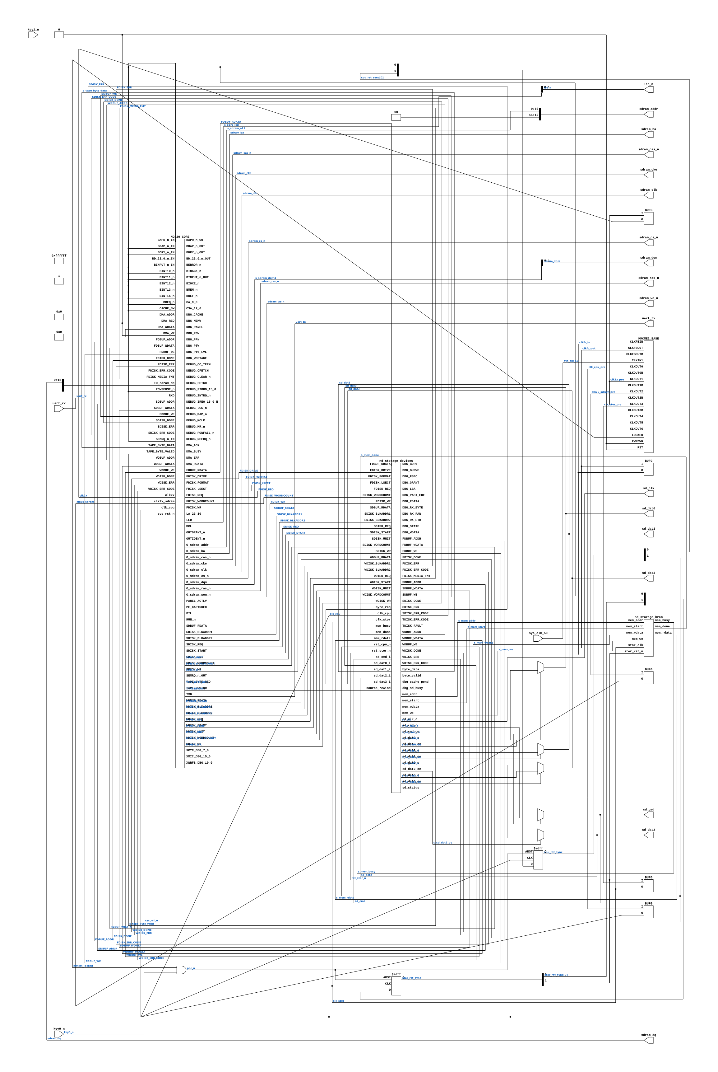
Contains: BUFG (vendor) x5, MMCME2_BASE (vendor), ND120_CORE, nd_storage_bram, nd_storage_devices
Module hierarchy - All modules
Schematic
Drawn from the Verilog: the yosys netlist of the QMTECH XC7A35T build, where it is the top. Sub-modules are boxes (click the picture to open it full size; there every sub-module box links to its page, and every wire shows its Verilog name).
Description
QMTECH XC7A35T SDRAM core board - ND-120 top level Full path: Verilog/fpga/qmtech-a35t/rtl/nd120_qmtech_top.v Written 04-SEP-2026. NOT YET BUILT OR RUN ON HARDWARE. WHAT THIS BOARD IS FOR The same XC7A35T die as the Basys3, but with a 32 MB SDRAM chip beside it. The Basys3 cannot run SINTRAN for want of memory - 100 RAMB18 gives 24 KB of main store - and that is a capacity limit no clock speed fixes. This board removes it. SHAPE OF THE BUILD Modelled on fpga/mega65/rtl/nd120_mega65_machine.v (the same CPU core and the same 16-bit SDRAM bridge mode, on the same Artix-7 fabric and the same Vivado flow) with the card-side storage taken from the Tang top (fpga/tang-nano-20k/src/ND120_TANG20K_TOP.v). It instantiates ND120_CORE rather than ND120_TOP because the ND-BUS device chain - papertape, floppy, Winchester - exists only on the core. MAIN MEMORY: 4 MB, the board's W9825G6KH-6 through the sheet-49 bridge (MEM_RAM_49_SDRAM + sdram18) in its 16-BIT module mode, ND_SDRAM_PACK16 + ND_SDRAM_DQ16. That is the configuration that boots SINTRAN on the MiSTer and builds timing-clean for the MEGA65 R6; this chip is 16 bits wide like the DE10-Nano module, so it needs the same mode. The mode maps 2M words as BANK0 + BANK2, which is the whole of the ND-120's onboard memory space: the CPU board's own decode puts onboard memory in the bottom 2M words (PAL_44445B.v:85), so the other 28 MB of the chip could not be addressed as main store however it were wired. REFRESH: this chip has 8192 rows and needs an auto-refresh every 7.8 us at most, so the build sets ND_SDRAM_REFRESH_US=7 - the same value the MiSTer uses for the same reason. The bridge's 15 us default suits the Tang's 2K-row die and would UNDER-refresh this one. STORAGE: SD card on the header, images served by nd_storage_devices, every client DIRECT (uncached). The region behind its mem_* port is a block RAM here (rtl/nd_storage_bram.v) rather than a slice of the SDRAM, because the 16-bit bridge mode has no working 32-bit access and the SDRAM device port needs one - the long version of that is in the header of nd_storage_bram.v. Uncached is a proven configuration, not a stopgap that has never run: the Tang served every disc that way for weeks, and the 23-AUG-2026 experiment measured no functional difference between cache on, cache masked off, and cache not synthesized. It costs speed, not function. Restoring the cache means teaching the 16-bit mode a two-beat 32-bit access; until then this build must be compiled with ND_STORAGE_NO_CACHE (build.tcl passes it). CONSOLE: the CPU's own serial pins, straight out to two header pins for a 3.3 V USB-serial adapter. 115200. There is no terminal core and no video on this board, so the glyphs are the PC terminal's problem. The board has NO on-board USB-UART - the Mini USB socket is power only. CLOCKS - one MMCM, VCO 1000 MHz from the 50 MHz oscillator: clk_cpu 1000/50 = 20.000 MHz CPU, bus, OSC, the device chain clk2x 1000/25 = 40.000 MHz the SDRAM bridge clk2x_sdram 1000/25 = 40.000 MHz at 180 degrees, to the chip's pin clk_stor 1000/37 = 27.027 MHz the SD/FAT stack clk2x is an exact integer 2x of clk_cpu off the same VCO, which is what the bridge's "same PLL, edge-aligned" rule requires. clk_stor is 27 MHz because the SD identification clock has to land in the card's legal 100-400 kHz window after the stack's own divisor, exactly as on the Tang and the Nexys - it is NOT a free choice. Ronny Hansen
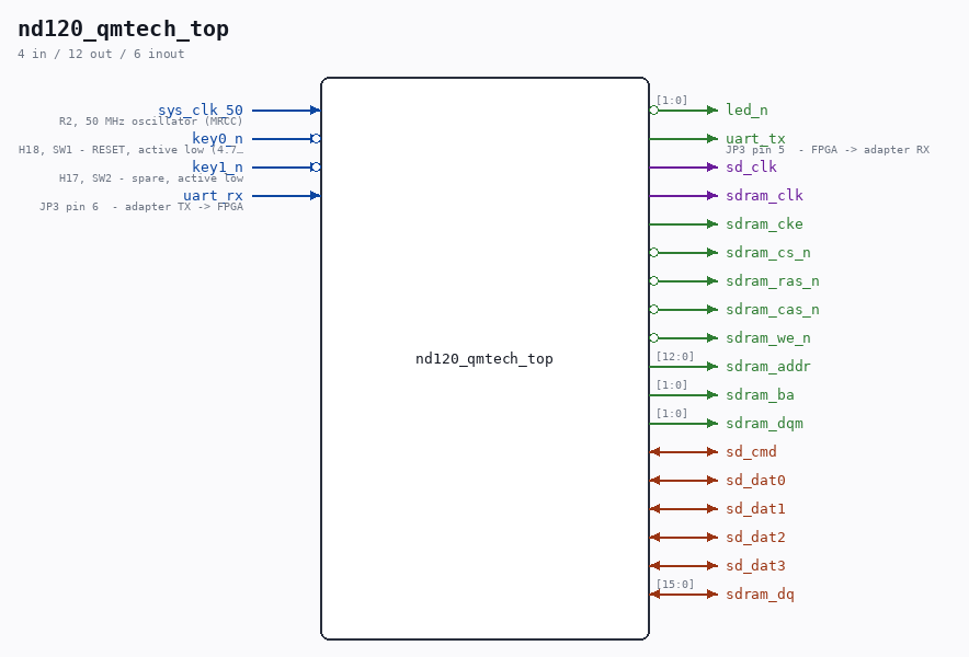
Ports
| Direction | Width | Name | Description |
|---|---|---|---|
| input | 1 |
sys_clk_50 |
R2, 50 MHz oscillator (MRCC) |
| input | 1 |
key0_n (active low) |
H18, SW1 - RESET, active low (4.7k pull-up) |
| input | 1 |
key1_n (active low) |
H17, SW2 - spare, active low |
| output | [1:0] |
led_n (active low) |
|
| input | 1 |
uart_rx |
JP3 pin 6 - adapter TX -> FPGA |
| output | 1 |
uart_tx |
JP3 pin 5 - FPGA -> adapter RX |
| output | 1 |
sd_clk |
|
| inout | 1 |
sd_cmd |
|
| inout | 1 |
sd_dat0 |
|
| inout | 1 |
sd_dat1 |
|
| inout | 1 |
sd_dat2 |
|
| inout | 1 |
sd_dat3 |
|
| output | 1 |
sdram_clk |
|
| output | 1 |
sdram_cke |
|
| output | 1 |
sdram_cs_n (active low) |
|
| output | 1 |
sdram_ras_n (active low) |
|
| output | 1 |
sdram_cas_n (active low) |
|
| output | 1 |
sdram_we_n (active low) |
|
| output | [12:0] |
sdram_addr |
|
| output | [1:0] |
sdram_ba |
|
| output | [1:0] |
sdram_dqm |
|
| inout | [15:0] |
sdram_dq |
Verilog source
Verilog/fpga/qmtech-a35t/rtl/nd120_qmtech_top.v on GitHub.
Show the Verilog of nd120_qmtech_top (579 lines)
/****************************************************************************
** QMTECH XC7A35T SDRAM core board - ND-120 top level **
** **
** Full path: Verilog/fpga/qmtech-a35t/rtl/nd120_qmtech_top.v **
** **
** Written 04-SEP-2026. NOT YET BUILT OR RUN ON HARDWARE. **
** **
** WHAT THIS BOARD IS FOR **
** The same XC7A35T die as the Basys3, but with a 32 MB SDRAM chip beside **
** it. The Basys3 cannot run SINTRAN for want of memory - 100 RAMB18 gives **
** 24 KB of main store - and that is a capacity limit no clock speed **
** fixes. This board removes it. **
** **
** SHAPE OF THE BUILD **
** Modelled on fpga/mega65/rtl/nd120_mega65_machine.v (the same CPU core **
** and the same 16-bit SDRAM bridge mode, on the same Artix-7 fabric and **
** the same Vivado flow) with the card-side storage taken from the Tang **
** top (fpga/tang-nano-20k/src/ND120_TANG20K_TOP.v). It instantiates **
** ND120_CORE rather than ND120_TOP because the ND-BUS device chain - **
** papertape, floppy, Winchester - exists only on the core. **
** **
** MAIN MEMORY: 4 MB, the board's W9825G6KH-6 through the sheet-49 bridge **
** (MEM_RAM_49_SDRAM + sdram18) in its 16-BIT module mode, ND_SDRAM_PACK16 **
** + ND_SDRAM_DQ16. That is the configuration that boots SINTRAN on the **
** MiSTer and builds timing-clean for the MEGA65 R6; this chip is 16 bits **
** wide like the DE10-Nano module, so it needs the same mode. The mode **
** maps 2M words as BANK0 + BANK2, which is the whole of the ND-120's **
** onboard memory space: the CPU board's own decode puts onboard memory in **
** the bottom 2M words (PAL_44445B.v:85), so the other 28 MB of the chip **
** could not be addressed as main store however it were wired. **
** **
** REFRESH: this chip has 8192 rows and needs an auto-refresh every 7.8 us **
** at most, so the build sets ND_SDRAM_REFRESH_US=7 - the same value the **
** MiSTer uses for the same reason. The bridge's 15 us default suits the **
** Tang's 2K-row die and would UNDER-refresh this one. **
** **
** STORAGE: SD card on the header, images served by nd_storage_devices, **
** every client DIRECT (uncached). The region behind its mem_* port is a **
** block RAM here (rtl/nd_storage_bram.v) rather than a slice of the **
** SDRAM, because the 16-bit bridge mode has no working 32-bit access and **
** the SDRAM device port needs one - the long version of that is in the **
** header of nd_storage_bram.v. Uncached is a proven configuration, not a **
** stopgap that has never run: the Tang served every disc that way for **
** weeks, and the 23-AUG-2026 experiment measured no functional difference **
** between cache on, cache masked off, and cache not synthesized. It costs **
** speed, not function. Restoring the cache means teaching the 16-bit mode **
** a two-beat 32-bit access; until then this build must be compiled with **
** ND_STORAGE_NO_CACHE (build.tcl passes it). **
** **
** CONSOLE: the CPU's own serial pins, straight out to two header pins for **
** a 3.3 V USB-serial adapter. 115200. There is no terminal core and no **
** video on this board, so the glyphs are the PC terminal's problem. The **
** board has NO on-board USB-UART - the Mini USB socket is power only. **
** **
** CLOCKS - one MMCM, VCO 1000 MHz from the 50 MHz oscillator: **
** clk_cpu 1000/50 = 20.000 MHz CPU, bus, OSC, the device chain **
** clk2x 1000/25 = 40.000 MHz the SDRAM bridge **
** clk2x_sdram 1000/25 = 40.000 MHz at 180 degrees, to the chip's pin **
** clk_stor 1000/37 = 27.027 MHz the SD/FAT stack **
** clk2x is an exact integer 2x of clk_cpu off the same VCO, which is what **
** the bridge's "same PLL, edge-aligned" rule requires. clk_stor is 27 MHz **
** because the SD identification clock has to land in the card's legal **
** 100-400 kHz window after the stack's own divisor, exactly as on the **
** Tang and the Nexys - it is NOT a free choice. **
** **
** Ronny Hansen **
*****************************************************************************/
`default_nettype none
module nd120_qmtech_top (
input wire sys_clk_50, //! R2, 50 MHz oscillator (MRCC)
input wire key0_n, //! H18, SW1 - RESET, active low (4.7k pull-up)
input wire key1_n, //! H17, SW2 - spare, active low
//! Two user LEDs, ACTIVE LOW (3V3 -> 1k -> LED -> pin, so 0 = lit).
//! led_n[0] = USER_LED0 = D8, led_n[1] = USER_LED1 = C8.
output wire [ 1:0] led_n,
//! Console to an external 3.3 V USB-serial adapter, on header JP3.
input wire uart_rx, //! JP3 pin 6 - adapter TX -> FPGA
output wire uart_tx, //! JP3 pin 5 - FPGA -> adapter RX
//! SD card (Pmod or breakout) on header JP3 pins 7-12.
output wire sd_clk,
inout wire sd_cmd,
inout wire sd_dat0,
inout wire sd_dat1,
inout wire sd_dat2,
inout wire sd_dat3,
//! Winbond W9825G6KH-6, 32 MB, 16-bit bus. Pin map: board-pins.xdc.
output wire sdram_clk,
output wire sdram_cke,
output wire sdram_cs_n,
output wire sdram_ras_n,
output wire sdram_cas_n,
output wire sdram_we_n,
output wire [12:0] sdram_addr,
output wire [ 1:0] sdram_ba,
output wire [ 1:0] sdram_dqm,
inout wire [15:0] sdram_dq
);
/**************************************************************************
* Clocks *
**************************************************************************/
wire clk_cpu_pre, clk2x_pre, clk2x_sdram_pre, clk_stor_pre;
wire clk_cpu, clk2x, clk2x_sdram, clk_stor;
wire clkfb_out, clkfb_in, mmcm_locked;
MMCME2_BASE #(
.BANDWIDTH ("OPTIMIZED"),
.CLKFBOUT_MULT_F (20.0), // VCO = 50 x 20 = 1000 MHz (600-1200 legal)
.CLKIN1_PERIOD (20.0), // 50 MHz
.CLKOUT0_DIVIDE_F(50.0), // 20.000 MHz - CPU and bus
.CLKOUT1_DIVIDE (25), // 40.000 MHz - SDRAM bridge (exactly 2x CPU)
.CLKOUT2_DIVIDE (25), // 40.000 MHz - SDRAM chip pin
.CLKOUT2_PHASE (180.0), // ...half a period late, as sdram18 requires
.CLKOUT3_DIVIDE (37), // 27.027 MHz - SD/FAT stack
.DIVCLK_DIVIDE (1),
.STARTUP_WAIT ("FALSE")
) MMCM (
.CLKIN1 (sys_clk_50),
.CLKFBIN (clkfb_in),
.CLKFBOUT(clkfb_out),
.CLKOUT0 (clk_cpu_pre),
.CLKOUT1 (clk2x_pre),
.CLKOUT2 (clk2x_sdram_pre),
.CLKOUT3 (clk_stor_pre),
.CLKOUT4 (),
.CLKOUT5 (),
.CLKOUT6 (),
.CLKOUT0B(),
.CLKOUT1B(),
.CLKOUT2B(),
.CLKOUT3B(),
.CLKFBOUTB(),
.LOCKED (mmcm_locked),
.PWRDWN (1'b0),
.RST (1'b0)
);
BUFG bufg_fb (.I(clkfb_out), .O(clkfb_in));
BUFG bufg_cpu (.I(clk_cpu_pre), .O(clk_cpu));
BUFG bufg_2x (.I(clk2x_pre), .O(clk2x));
BUFG bufg_2xsd (.I(clk2x_sdram_pre), .O(clk2x_sdram));
BUFG bufg_stor (.I(clk_stor_pre), .O(clk_stor));
/**************************************************************************
* Reset *
* *
* One source: the MMCM lock ANDed with the reset key (active low, so *
* pressed = 0 = held in reset). It is released into each clock domain *
* through its own two-flop synchroniser - asserted asynchronously, *
* released synchronously - so no domain sees a reset edge that misses *
* its setup window. *
**************************************************************************/
wire por_n = mmcm_locked & key0_n;
reg [1:0] cpu_rst_sync = 2'b00;
always @(posedge clk_cpu or negedge por_n)
if (!por_n) cpu_rst_sync <= 2'b00;
else cpu_rst_sync <= {cpu_rst_sync[0], 1'b1};
wire sys_rst_n = cpu_rst_sync[1];
reg [1:0] stor_rst_sync = 2'b00;
always @(posedge clk_stor or negedge por_n)
if (!por_n) stor_rst_sync <= 2'b00;
else stor_rst_sync <= {stor_rst_sync[0], 1'b1};
wire rst_stor_n = stor_rst_sync[1];
/**************************************************************************
* Storage: the three controller seams served from the SD card *
**************************************************************************/
// tape (client 0)
wire TAPE_BYTE_REQ, TAPE_REWIND;
wire s_tape_byte_valid;
wire [ 7:0] s_tape_byte_data;
wire TDISK_FAULT;
wire [ 3:0] TDISK_ERR_CODE;
// floppy (client 1)
wire FDISK_REQ, FDISK_WR, FDISK_DONE, FDISK_ERR, FDBUF_WE;
wire [15:0] FDISK_LSECT, FDBUF_WDATA, FDBUF_RDATA;
wire [ 1:0] FDISK_FORMAT, FDISK_DRIVE;
wire [10:0] FDISK_WORDCOUNT;
wire [ 3:0] FDISK_ERR_CODE, FDISK_MEDIA_FMT;
wire [ 9:0] FDBUF_ADDR;
// SMD (client 3) - not built on this board, but the seam is wired through
// because both ends declare it unconditionally. INCLUDE_SMD=0 on both, so
// nothing drives it.
wire SDISK_START, SDISK_REQ, SDISK_WR, SDISK_DONE, SDISK_ERR, SDBUF_WE;
wire [15:0] SDISK_BLKADDR1, SDISK_BLKADDR2, SDBUF_WDATA, SDBUF_RDATA;
wire [ 2:0] SDISK_UNIT;
wire [10:0] SDISK_WORDCOUNT;
wire [ 3:0] SDISK_ERR_CODE;
wire [ 9:0] SDBUF_ADDR;
// Winchester (client 6)
wire WDISK_START, WDISK_REQ, WDISK_WR, WDISK_DONE, WDISK_ERR, WDBUF_WE;
wire [15:0] WDISK_BLKADDR1, WDISK_BLKADDR2, WDBUF_WDATA, WDBUF_RDATA;
wire [ 2:0] WDISK_UNIT;
wire [10:0] WDISK_WORDCOUNT;
wire [ 3:0] WDISK_ERR_CODE;
wire [ 9:0] WDBUF_ADDR;
// SD pins: driven through explicit output-enables so the tri-state is a
// real IOBUF. The 'z' must be the OUTER branch of the ternary - a 'z' in an
// inner branch is silently dropped by some tool chains (the note at
// ND120_TANG20K_TOP.v:2140 was learned the hard way).
wire s_sd_clk_o;
wire s_sd_cmd_o, s_sd_cmd_oe;
wire s_sd_dat0_o, s_sd_dat0_oe;
wire s_sd_dat1_o, s_sd_dat1_oe;
wire s_sd_dat2_o, s_sd_dat2_oe;
wire s_sd_dat3_o, s_sd_dat3_oe;
/* verilator lint_off UNUSEDSIGNAL */
wire [1:0] s_sd_status;
wire s_dbg_sd_busy, s_dbg_cache_pend;
/* verilator lint_on UNUSEDSIGNAL */
assign sd_clk = s_sd_clk_o;
assign sd_cmd = s_sd_cmd_oe ? s_sd_cmd_o : 1'bz;
assign sd_dat0 = s_sd_dat0_oe ? s_sd_dat0_o : 1'bz;
assign sd_dat1 = s_sd_dat1_oe ? s_sd_dat1_o : 1'bz;
assign sd_dat2 = s_sd_dat2_oe ? s_sd_dat2_o : 1'bz;
assign sd_dat3 = s_sd_dat3_oe ? s_sd_dat3_o : 1'bz;
// the region behind nd_storage's mem_* port
wire s_mem_start, s_mem_we, s_mem_busy, s_mem_done;
wire [19:0] s_mem_addr;
wire [31:0] s_mem_wdata, s_mem_rdata;
nd_storage_devices #(
// 1-BIT first. The card sits on jumper wires to a 2.54 mm header here,
// not on a short board trace like the Tang's slot, so the 4-bit bus is
// a second variable to introduce only once 1-bit reads are proven.
// The pins for it are wired and constrained, so it is a parameter flip.
.USE_4BIT (0),
.SIMULATE (0), // real card: full-length SD init
.INCLUDE_TAPE (1),
.INCLUDE_FLOPPY(1),
.INCLUDE_SMD (0),
.INCLUDE_WD (1),
// BOOT.TAP, not the default BOOT.BPUN: a 4-character extension needs a
// VFAT long-filename entry, and builds that carry the floppy and the
// Winchester strip long-filename parsing (SDFAT_NO_LFN) to save LUTs.
// An 8.3 name is readable by every build variant.
.BOOT_NAME ("BOOT.TAP"),
.BOOT_LEN (8'd8)
) STORAGE (
.clk_stor (clk_stor),
.rst_stor_n(rst_stor_n),
.clk_cpu (clk_cpu),
.rst_cpu_n (sys_rst_n),
.byte_req (TAPE_BYTE_REQ),
.byte_valid (s_tape_byte_valid),
.byte_data (s_tape_byte_data),
.source_rewind (TAPE_REWIND),
.TDISK_FAULT (TDISK_FAULT),
.TDISK_ERR_CODE(TDISK_ERR_CODE),
.FDISK_REQ (FDISK_REQ),
.FDISK_WR (FDISK_WR),
.FDISK_LSECT (FDISK_LSECT),
.FDISK_FORMAT (FDISK_FORMAT),
.FDISK_DRIVE (FDISK_DRIVE),
.FDISK_WORDCOUNT(FDISK_WORDCOUNT),
.FDISK_DONE (FDISK_DONE),
.FDISK_ERR (FDISK_ERR),
.FDISK_ERR_CODE (FDISK_ERR_CODE),
.FDISK_MEDIA_FMT(FDISK_MEDIA_FMT),
.FDBUF_ADDR (FDBUF_ADDR),
.FDBUF_WDATA (FDBUF_WDATA),
.FDBUF_WE (FDBUF_WE),
.FDBUF_RDATA (FDBUF_RDATA),
.SDISK_START (SDISK_START),
.SDISK_REQ (SDISK_REQ),
.SDISK_WR (SDISK_WR),
.SDISK_BLKADDR1 (SDISK_BLKADDR1),
.SDISK_BLKADDR2 (SDISK_BLKADDR2),
.SDISK_UNIT (SDISK_UNIT),
.SDISK_WORDCOUNT(SDISK_WORDCOUNT),
.SDISK_DONE (SDISK_DONE),
.SDISK_ERR (SDISK_ERR),
.SDISK_ERR_CODE (SDISK_ERR_CODE),
.SDBUF_ADDR (SDBUF_ADDR),
.SDBUF_WDATA (SDBUF_WDATA),
.SDBUF_WE (SDBUF_WE),
.SDBUF_RDATA (SDBUF_RDATA),
.WDISK_START (WDISK_START),
.WDISK_REQ (WDISK_REQ),
.WDISK_WR (WDISK_WR),
.WDISK_BLKADDR1 (WDISK_BLKADDR1),
.WDISK_BLKADDR2 (WDISK_BLKADDR2),
.WDISK_UNIT (WDISK_UNIT),
.WDISK_WORDCOUNT(WDISK_WORDCOUNT),
.WDISK_DONE (WDISK_DONE),
.WDISK_ERR (WDISK_ERR),
.WDISK_ERR_CODE (WDISK_ERR_CODE),
.WDBUF_ADDR (WDBUF_ADDR),
.WDBUF_WDATA (WDBUF_WDATA),
.WDBUF_WE (WDBUF_WE),
.WDBUF_RDATA (WDBUF_RDATA),
.sd_clk_o (s_sd_clk_o),
.sd_cmd_i (sd_cmd),
.sd_cmd_o (s_sd_cmd_o),
.sd_cmd_oe (s_sd_cmd_oe),
.sd_dat0_i (sd_dat0),
.sd_dat0_o (s_sd_dat0_o),
.sd_dat0_oe(s_sd_dat0_oe),
.sd_dat1_i (sd_dat1),
.sd_dat1_o (s_sd_dat1_o),
.sd_dat1_oe(s_sd_dat1_oe),
.sd_dat2_i (sd_dat2),
.sd_dat2_o (s_sd_dat2_o),
.sd_dat2_oe(s_sd_dat2_oe),
.sd_dat3_i (sd_dat3),
.sd_dat3_o (s_sd_dat3_o),
.sd_dat3_oe(s_sd_dat3_oe),
.dbg_sd_busy (s_dbg_sd_busy),
.dbg_cache_pend(s_dbg_cache_pend),
.mem_start(s_mem_start),
.mem_we (s_mem_we),
.mem_addr (s_mem_addr),
.mem_wdata(s_mem_wdata),
.mem_rdata(s_mem_rdata),
.mem_busy (s_mem_busy),
.mem_done (s_mem_done),
.DBG_STATE (),
.DBG_LBA (),
.DBG_WDATA (),
.DBG_RDATA (),
.DBG_BUFW (),
.DBG_BUFWE (),
.DBG_FSEC (),
.DBG_RX_STB (),
.DBG_RX_RAW (),
.DBG_RX_BYTE (),
.DBG_PAST_EOF(),
.DBG_GRANT (),
.sd_status (s_sd_status)
);
// The region itself. One staging line is all an all-DIRECT build touches;
// see the header of nd_storage_bram.v for why it is block RAM here and not
// a slice of the SDRAM as on the Tang.
nd_storage_bram #(
.WORDS(1024)
) STORAGE_REGION (
.stor_clk (clk_stor),
.stor_rst_n(rst_stor_n),
.mem_start (s_mem_start),
.mem_we (s_mem_we),
.mem_addr (s_mem_addr),
.mem_wdata (s_mem_wdata),
.mem_rdata (s_mem_rdata),
.mem_busy (s_mem_busy),
.mem_done (s_mem_done)
);
/**************************************************************************
* Main memory pin adaptation *
* *
* The bridge's ports are the Tang's 32-bit shape. On a 16-bit module the *
* upper 16 DQ bits and the upper 2 DQM bits go nowhere, and the bridge *
* drives 11 address lines against this chip's 13 - the top two are 0, *
* which is what confines main memory to the 2K rows x 256 columns x 4 *
* banks the DQ16 mode maps. Same adaptation as nd120.sv (MiSTer) and *
* nd120_mega65_machine.v. *
**************************************************************************/
/* verilator lint_off UNUSEDSIGNAL */
wire [15:0] s_sdram_dq_hi; // bridge DQ[31:16]: not a pin, not read
/* verilator lint_on UNUSEDSIGNAL */
wire [10:0] s_sdram_a11;
wire [ 3:0] s_sdram_dqm4;
assign sdram_addr = {2'b00, s_sdram_a11};
assign sdram_dqm = s_sdram_dqm4[1:0];
/**************************************************************************
* The ND-120 CPU board *
**************************************************************************/
// No external ND bus on this board: the same tie-offs the Tang, MiSTer and
// MEGA65 use. The bus is pulled to its idle (all ones = inactive) state.
wire [23:0] s_bd_in = 24'hFFFFFF;
wire [ 6:0] s_core_led;
wire s_core_run_n;
ND120_CORE #(
.INCLUDE_TAPE (1),
.INCLUDE_FLOPPY(1),
.INCLUDE_SMD (0),
.INCLUDE_WD (1)
) CORE (
.clk_cpu (clk_cpu),
.sys_rst_n(sys_rst_n),
// The CPU's own cache. Left ON: this part has the block RAM for it,
// unlike the Tang where it does not fit.
.CACHE_SW (1'b1),
.BREQ_n (1'b1),
.BINT10_n (1'b1),
.BINT11_n (1'b1),
.BINT12_n (1'b1),
.BINT13_n (1'b1),
.BINT15_n (1'b1),
.POWSENSE_n(1'b1),
.BD_23_0_n_IN (s_bd_in),
.BD_23_0_n_OUT(),
.SEMRQ_n_IN (1'b1),
.SEMRQ_n_OUT(),
.BINPUT_n_IN (1'b1),
.BINPUT_n_OUT(),
.BDAP_n_IN (1'b1),
.BDAP_n_OUT(),
.BDRY_n_IN (1'b1),
.BDRY_n_OUT(),
.BAPR_n_IN (1'b1),
.BAPR_n_OUT(),
.BREF_n (),
.BERROR_n (),
.BINACK_n (),
.BIOXE_n (),
.BMEM_n (),
.OUTGRANT_n(),
.OUTIDENT_n(),
.MCL (),
// The console: the CPU's serial pins go straight to the header.
.RXD(uart_rx),
.TXD(uart_tx),
.TAPE_BYTE_REQ (TAPE_BYTE_REQ),
.TAPE_BYTE_VALID(s_tape_byte_valid),
.TAPE_BYTE_DATA (s_tape_byte_data),
.TAPE_REWIND (TAPE_REWIND),
.DMA_REQ (1'b0),
.DMA_WR (1'b0),
.DMA_ADDR (24'd0),
.DMA_WDATA(16'd0),
.DMA_RDATA(),
.DMA_ACK (),
.DMA_ERR (),
.DMA_BUSY (),
.FDISK_REQ (FDISK_REQ),
.FDISK_WR (FDISK_WR),
.FDISK_LSECT (FDISK_LSECT),
.FDISK_FORMAT (FDISK_FORMAT),
.FDISK_DRIVE (FDISK_DRIVE),
.FDISK_WORDCOUNT(FDISK_WORDCOUNT),
.FDISK_DONE (FDISK_DONE),
.FDISK_ERR (FDISK_ERR),
.FDISK_ERR_CODE (FDISK_ERR_CODE),
.FDISK_MEDIA_FMT(FDISK_MEDIA_FMT),
.FDBUF_ADDR (FDBUF_ADDR),
.FDBUF_WDATA (FDBUF_WDATA),
.FDBUF_WE (FDBUF_WE),
.FDBUF_RDATA (FDBUF_RDATA),
.SDISK_START (SDISK_START),
.SDISK_REQ (SDISK_REQ),
.SDISK_WR (SDISK_WR),
.SDISK_BLKADDR1 (SDISK_BLKADDR1),
.SDISK_BLKADDR2 (SDISK_BLKADDR2),
.SDISK_UNIT (SDISK_UNIT),
.SDISK_WORDCOUNT(SDISK_WORDCOUNT),
.SDISK_DONE (SDISK_DONE),
.SDISK_ERR (SDISK_ERR),
.SDISK_ERR_CODE (SDISK_ERR_CODE),
.SDBUF_ADDR (SDBUF_ADDR),
.SDBUF_WDATA (SDBUF_WDATA),
.SDBUF_WE (SDBUF_WE),
.SDBUF_RDATA (SDBUF_RDATA),
.WDISK_START (WDISK_START),
.WDISK_REQ (WDISK_REQ),
.WDISK_WR (WDISK_WR),
.WDISK_BLKADDR1 (WDISK_BLKADDR1),
.WDISK_BLKADDR2 (WDISK_BLKADDR2),
.WDISK_UNIT (WDISK_UNIT),
.WDISK_WORDCOUNT(WDISK_WORDCOUNT),
.WDISK_DONE (WDISK_DONE),
.WDISK_ERR (WDISK_ERR),
.WDISK_ERR_CODE (WDISK_ERR_CODE),
.WDBUF_ADDR (WDBUF_ADDR),
.WDBUF_WDATA (WDBUF_WDATA),
.WDBUF_WE (WDBUF_WE),
.WDBUF_RDATA (WDBUF_RDATA),
// SDRAM main memory (MAIN_RAM_SDRAM, threaded down to MEM_RAM_49_SDRAM)
.clk2x (clk2x),
.clk2x_sdram (clk2x_sdram),
.O_sdram_clk (sdram_clk),
.O_sdram_cke (sdram_cke),
.O_sdram_cs_n (sdram_cs_n),
.O_sdram_cas_n(sdram_cas_n),
.O_sdram_ras_n(sdram_ras_n),
.O_sdram_wen_n(sdram_we_n),
.IO_sdram_dq ({s_sdram_dq_hi, sdram_dq}),
.O_sdram_addr (s_sdram_a11),
.O_sdram_ba (sdram_ba),
.O_sdram_dqm (s_sdram_dqm4),
.DBG_MEMW (),
.DBG_PTW (),
.PF_CAPTURED (),
.DBG_WDSTAGE (),
.DBG_PPN (),
.DBG_PGW (),
.LED (s_core_led),
.RUN_n (s_core_run_n),
.CSA_12_0 (),
.PIL (),
.LA_23_10 (),
.CA_9_0 (),
.DEBUG_CC_TERM (),
.DEBUG_MCLK (),
.DEBUG_LCS_n (),
.DEBUG_FETCH (),
.DEBUG_MAP_n (),
.DEBUG_CFETCH (),
.DEBUG_MR_n (),
.DEBUG_CLEAR_n (),
.DEBUG_REFRQ_n (),
.DEBUG_INTRQ_n (),
.DEBUG_POWFAIL_n (),
.DEBUG_FIDBO_15_0(),
.DEBUG_IREQ_15_0_N(),
.XMIC_DBG_15_0 (),
.XWRFB_DBG_19_0 (),
.XCYC_DBG_7_0 (),
.DBG_PTW_LVL (),
.DBG_PANEL (),
.PANEL_ACTLV (),
.DBG_CACHE ()
);
/**************************************************************************
* LEDs *
* *
* BOTH SIDES ARE ACTIVE LOW, so these pass straight through with no *
* inversion. The CPU board's own lamps are active low at the source *
* (IO_REG_41.v, measured on the MiSTer), and this board's LEDs are *
* 3V3 -> 1k -> LED -> pin, so driving 0 lights them. A wrapper that *
* inverts here would show both lamps backwards - which is exactly what *
* happened once on a board where only one side was active low. *
* led_n[0] = D8 = CPU RED (error / halt) *
* led_n[1] = C8 = CPU GREEN (self-test passed, running) *
**************************************************************************/
assign led_n[0] = s_core_led[0];
assign led_n[1] = s_core_led[1];
// Named so lint does not report them as dropped: the board has only two
// LEDs, and key1 has no function in this build.
/* verilator lint_off UNUSEDSIGNAL */
wire [4:0] s_led_unused = s_core_led[6:2];
wire s_run_unused = s_core_run_n;
wire s_key1_unused = key1_n;
/* verilator lint_on UNUSEDSIGNAL */
endmodule
`default_nettype wire