CGA_MIC_MASEL_REPEAT
Source: Verilog/DELILAH-CPU/CGA_MIC/circuit/CGA_MIC_MASEL_REPEAT.v
Hierarchy: not instantiated by any of the 9 build tops (elaborated by yosys).
Module hierarchy - All modules
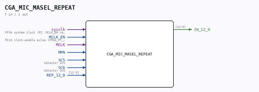
Schematic
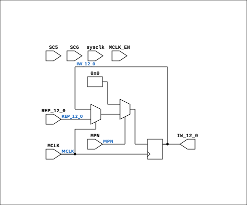
Drawn from the Verilog: no build top uses this module, so it was elaborated from its own file with no defines and default parameters. Sub-modules are boxes (click the picture to open it full size; there every sub-module box links to its page, and every wire shows its Verilog name).
Description
ND120 CGA (CPU Gate Array / DELILAH) /CGA/MIC/MASEL/REPEAT REPEAT Page 20 SHEET 1 of 1 Last reviewed: 1-DEC-2024 Ronny Hansen
Ports
| Direction | Width | Name | Description |
|---|---|---|---|
| input | 1 |
sysclk |
FPGA system clock (P2: MCLK_EN capture) |
| input | 1 |
MCLK_EN |
MCLK clock-enable pulse (FPGA_FF_MODE, else 0) |
| input | 1 |
MCLK |
|
| input | 1 |
MPN |
|
| input | 1 |
SC5 |
Selector SC5 |
| input | 1 |
SC6 |
Selector SC6 |
| input | [12:0] |
REP_12_0 |
|
| output | [12:0] |
IW_12_0 |
Verilog source
Verilog/DELILAH-CPU/CGA_MIC/circuit/CGA_MIC_MASEL_REPEAT.v on GitHub.
Show the Verilog of CGA_MIC_MASEL_REPEAT (126 lines)
/**************************************************************************
** ND120 CGA (CPU Gate Array / DELILAH)                                  **
** /CGA/MIC/MASEL/REPEAT                                                 **
** REPEAT                                                                **
**                                                                       **
** Page 20                                                               **
** SHEET 1 of 1                                                          **
**                                                                       **
** Last reviewed: 1-DEC-2024                                             **
** Ronny Hansen                                                          **
***************************************************************************/

module CGA_MIC_MASEL_REPEAT (
    input        sysclk,   //! FPGA system clock (P2: MCLK_EN capture)
    input        MCLK_EN,  //! MCLK clock-enable pulse (FPGA_FF_MODE, else 0)

    input        MCLK,
    input        MPN,
    input        SC5,      //! Selector SC5
    input        SC6,      //! Selector SC6
    input [12:0] REP_12_0,

    output [12:0] IW_12_0
);

  /*******************************************************************************
   ** The wires are defined here                                                 **
   *******************************************************************************/
  wire [12:0] s_rep_12_0;
  wire        s_mclk;
  wire        s_mp_n;
  wire        s_mp;
  wire        s_sc5;
  wire        s_sc6;

  /*******************************************************************************
   ** The module functionality is described here                                 **
   *******************************************************************************/
  reg  [12:0] regRepeat;


  /*******************************************************************************
   ** Here all input connections are defined                                     **
   *******************************************************************************/
  assign s_rep_12_0[12:0] = REP_12_0;
  assign s_mp_n           = MPN;
  assign s_mclk           = MCLK;
  assign s_sc5            = SC5;
  assign s_sc6            = SC6;

  /*******************************************************************************
   ** Here all output connections are defined                                    **
   *******************************************************************************/
  assign IW_12_0          = regRepeat[12:0];

  /*******************************************************************************
   ** Here all in-lined components are defined                                   **
   *******************************************************************************/

  // NOT Gate
  assign s_mp             = ~s_mp_n;

  /*******************************************************************************
   ** Here all normal components are defined                                     **
   *******************************************************************************/

  // NOTE: Triggering on NEG edge is different from what the schematics say, but it is needed to get the R_REP value clocked correct

  wire s_hack;
  assign s_hack =
        s_mclk
        & !s_sc5
        & !s_sc6
        //& (regRepeat == 13'h1FFF | regRepeat == 13'h000)
        //& (REP_12_0 == 13'h401)

    ;// Latch if selector changes to jump and current regRepeat is 0. HACK HACK to get boot to work
/*
  always @(posedge s_mclk or posedge s_mp or posedge s_hack) begin
    if (s_mp) begin
      regRepeat <= 12'b000000000000;
    end else begin
      if (s_mclk) begin  // HACK: Allow changes in selector to affect the register values as long clock is high.. (to avoid race conditions)
        regRepeat[12:0] <= s_rep_12_0[12:0];
      end
    end
  end
*/

  // MCLK domain: regRepeat clocks on posedge s_mclk (s_mp is a sync clear).
  // P2 (docs/plan-fix-unconstrained-clocks.md): in FF mode capture on
  // posedge sysclk gated by MCLK_EN (aligned to the MCLK rise) instead
  // of clocking on the routed net. The original inner "if (s_mclk)"
  // guard is vacuously true at posedge s_mclk and is dropped here
  // (at the MCLK_EN capture edge the MCLK level register is still low).
`ifdef FPGA_FF_MODE
  always @(posedge sysclk) begin
    if (MCLK_EN) begin
      if (s_mp) begin
        regRepeat <= 12'b000000000000;
      end else begin
        regRepeat[12:0] <= s_rep_12_0[12:0];
      end
    end
  end
`else
  /* verilator lint_off UNUSEDSIGNAL */
  wire unused_en = sysclk & MCLK_EN;
  /* verilator lint_on UNUSEDSIGNAL */
  always @(posedge s_mclk) begin // or posedge s_mp) begin
    if (s_mp) begin
      regRepeat <= 12'b000000000000;
    end else begin
      if (s_mclk) begin
        regRepeat[12:0] <= s_rep_12_0[12:0];
      end
    end
  end
`endif


endmodule