CGA_MAC
Source: Verilog/DELILAH-CPU/CGA_MAC/circuit/CGA_MAC.v
Where it sits (Simulation): ND120_TOP > ND120_CORE > ND3202D > CPU_15 > CPU_PROC_32 > CPU_PROC_CGA_33 > CGA > CGA_MAC
- instance path: CORE.CPU_BOARD.CPU.PROC.CGA.DELILAH.MAC
Used in: CGA (all tops)
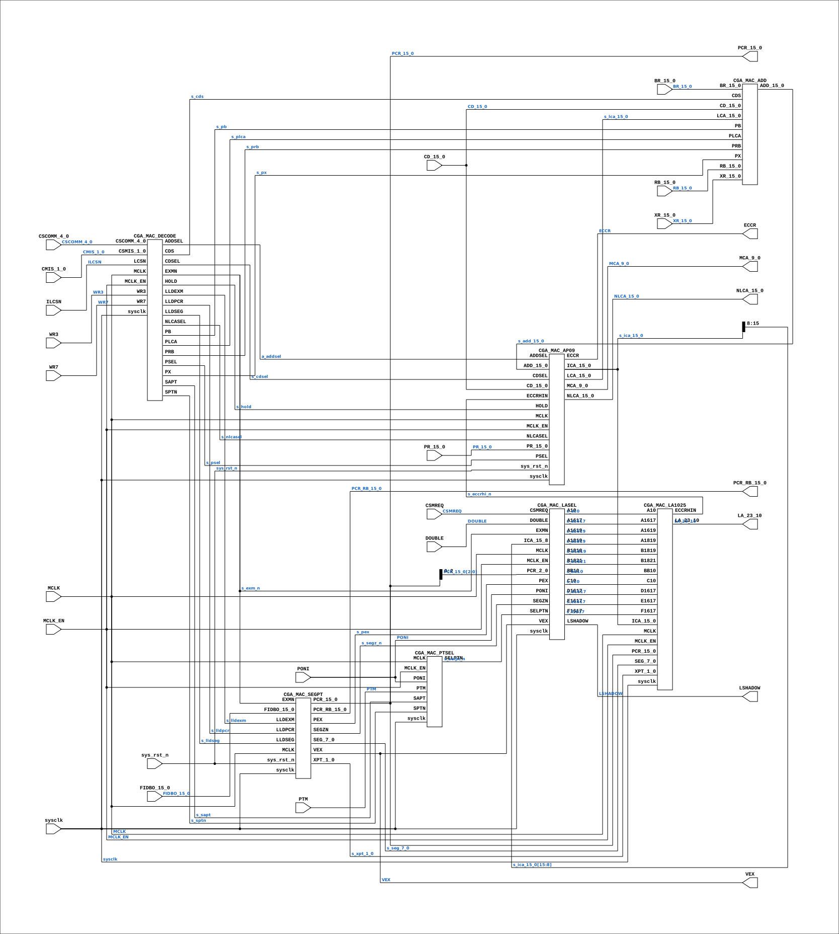
Contains: CGA_MAC_ADD, CGA_MAC_AP09, CGA_MAC_DECODE, CGA_MAC_LA1025, CGA_MAC_LASEL, CGA_MAC_PTSEL, CGA_MAC_SEGPT
Module hierarchy - All modules
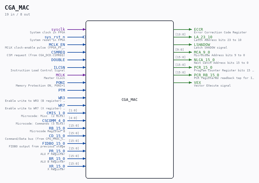
Schematic
Drawn from the Verilog: the yosys netlist of the Simulation (Verilator) build, instance CORE.CPU_BOARD.CPU.PROC.CGA.DELILAH.MAC. Sub-modules are boxes (click the picture to open it full size; there every sub-module box links to its page, and every wire shows its Verilog name).
Description
ND120 CGA (CPU Gate Array / DELILAH) /CGA/MAC MAC Page 24 SHEET 1 of 1 Last reviewed: 9-FEB-2025 Ronny Hansen
Ports
| Direction | Width | Name | Description |
|---|---|---|---|
| input | 1 |
sysclk |
System clock in FPGA |
| input | 1 |
sys_rst_n (active low) |
System reset in FPGA |
| input | 1 |
MCLK_EN |
MCLK clock-enable pulse (FPGA_FF_MODE, else 0) |
| input | 1 |
CSMREQ |
CSM request (from CGA_DCD.CSMREQ) |
| input | 1 |
DOUBLE |
|
| input | 1 |
ILCSN |
Instruction Load Control Signal |
| input | 1 |
MCLK |
Master CLock |
| input | 1 |
PONI |
Memory Protection ON, PONI=1 |
| input | 1 |
PTM |
|
| input | 1 |
WR3 |
Enable write to WR3 (B register) (from WR_15_0) (from CGA_WRF.WR3) |
| input | 1 |
WR7 |
Enable write to WR7 (X register) (from WR_15_0) (from CGA_WRF.WR7) |
| input | [1:0] |
CMIS_1_0 |
Microcode: Misc (2 bits) |
| input | [4:0] |
CSCOMM_4_0 |
Microcode: Commands (5 bits) |
| input | [15:0] |
RB_15_0 |
Microcode Register B |
| input | [15:0] |
CD_15_0 |
Command/Data bus (from CPU_PROC_CGA_33.CD_15_0) |
| input | [15:0] |
FIDBO_15_0 |
FIDBO output from previous stage |
| input | [15:0] |
PR_15_0 |
ALU P Register |
| input | [15:0] |
BR_15_0 |
ALU B Register |
| input | [15:0] |
XR_15_0 |
X Register |
| output | 1 |
ECCR |
Error Correction Code Register |
| output | [13:0] |
LA_23_10 |
Latch Address bits 23 to 10 |
| output | 1 |
LSHADOW |
Latch SHADOW signal |
| output | [9:0] |
MCA_9_0 |
Microcode Address bits 9 to 0 |
| output | [15:0] |
NLCA_15_0 |
Next Latch Address bits 15 to 0 |
| output | [15:0] |
PCR_15_0 |
Program Counter Register bits 15 to 0 |
| output | [15:0] |
PCR_RB_15_0 |
PCR registered readback tap for IDBCTL/SEL6 (IDB loop cut) |
| output | 1 |
VEX |
Vector EXecute signal |
Verilog source
Verilog/DELILAH-CPU/CGA_MAC/circuit/CGA_MAC.v on GitHub.
Show the Verilog of CGA_MAC (350 lines)
/**************************************************************************
** ND120 CGA (CPU Gate Array / DELILAH)                                  **
** /CGA/MAC                                                              **
** MAC                                                                   **
**                                                                       **
** Page 24                                                               **
** SHEET 1 of 1                                                          **
**                                                                       **
** Last reviewed: 9-FEB-2025                                             **
** Ronny Hansen                                                          **
***************************************************************************/

module CGA_MAC (
    // System input signals
    input sysclk,    // System clock in FPGA
    input sys_rst_n, // System reset in FPGA

    // Input signals
    input        MCLK_EN,     //! MCLK clock-enable pulse (FPGA_FF_MODE, else 0)
    input        CSMREQ,      //! CSM request (from CGA_DCD.CSMREQ)
    input        DOUBLE,
    input        ILCSN,       //! Instruction Load Control Signal
    input        MCLK,        //! Master CLock
    input        PONI,        //! Memory Protection ON, PONI=1
    input        PTM,
    input        WR3,         //! Enable write to WR3 (B register) (from WR_15_0) (from CGA_WRF.WR3)
    input        WR7,         //! Enable write to WR7 (X register) (from WR_15_0) (from CGA_WRF.WR7)
    input [ 1:0] CMIS_1_0,    //! Microcode: Misc  (2 bits)
    input [ 4:0] CSCOMM_4_0,  //! Microcode: Commands (5 bits)
    input [15:0] RB_15_0,     //! Microcode Register B
    input [15:0] CD_15_0,     //! Command/Data bus (from CPU_PROC_CGA_33.CD_15_0)
    input [15:0] FIDBO_15_0,  //! FIDBO output from previous stage
    input [15:0] PR_15_0,     //! ALU P Register
    input [15:0] BR_15_0,     //! ALU B Register
    input [15:0] XR_15_0,     //! X Register


    // Output signals
    output        ECCR,        //! Error Correction Code Register
    output [13:0] LA_23_10,    //! Latch Address bits 23 to 10
    output        LSHADOW,     //! Latch SHADOW signal
    output [ 9:0] MCA_9_0,     //! Microcode Address bits 9 to 0
    output [15:0] NLCA_15_0,   //! Next Latch Address bits 15 to 0
    output [15:0] PCR_15_0,    //! Program Counter Register bits 15 to 0
    output [15:0] PCR_RB_15_0, //! PCR registered readback tap for IDBCTL/SEL6 (IDB loop cut)
    output        VEX          //! Vector EXecute signal
);

  /*******************************************************************************
   ** The wires are defined here                                                 **
   *******************************************************************************/
  wire [ 1:0] s_cmis_1_0;
  wire [ 1:0] s_xpt_1_0;
  wire [ 4:0] s_cscomm_4_0;
  wire [ 7:0] s_seg_7_0;
  wire [ 9:0] s_mca_9_0_out;
  // ND120_ILA_MARK_DEBUG (Nexys build.tcl -tclargs ila): keep the three
  // address-chain nets through synthesis so the JTAG ILA can probe the
  // stages of the LIST-FILE-NAMES wrong-indirect-jump fault:
  //   s_cd_15_0 (memory data in) -> s_ica_15_0 (AP09 effective-address
  //   mux out) -> s_la_23_10_out (LA1025 physical address out).
  // No functional effect; the define is set only by that build flag.
`ifdef ND120_ILA_MARK_DEBUG
  (* mark_debug = "true" *)
`endif
  wire [13:0] s_la_23_10_out;
  wire [15:0] s_add_15_0;
  wire [15:0] s_br_15_0;
`ifdef ND120_ILA_MARK_DEBUG
  (* mark_debug = "true" *)
`endif
  wire [15:0] s_cd_15_0;
  wire [15:0] s_fidbo_15_0;
`ifdef ND120_ILA_MARK_DEBUG
  (* mark_debug = "true" *)
`endif
  wire [15:0] s_ica_15_0;
  wire [15:0] s_lca_15_0;
  wire [15:0] s_nlca_15_0_out;
  wire [15:0] s_pcr_15_0_out;
  wire [15:0] s_pr_15_0;
  wire [15:0] s_rb_15_0;
  wire [15:0] s_xr_15_0;

  wire        a_addsel;
  wire        s_a10;
  wire        s_a1617;
  wire        s_a1619;
  wire        s_a1819;
  wire        s_b1819;
  wire        s_b1821;
  wire        s_bb10;
  wire        s_c10;
  wire        s_cds;
  wire        s_cdsel;
  wire        s_csmreq;
  wire        s_d1617;
  wire        s_double;
  wire        s_e1617;
  wire        s_eccr_out;
  wire        s_eccrhi_n;
  wire        s_exm_n;
  wire        s_f1617;
  wire        s_hold;
  wire        s_ilcs_n;
  wire        s_ilcs;
  wire        s_lcs_n;
  wire        s_lldexm;
  wire        s_lldpcr;
  wire        s_lldseg;
  wire        s_lshadow_out;
  wire        s_mclk;
  wire        s_nlcasel;
  wire        s_pb;
  wire        s_pex;
  wire        s_plca;
  wire        s_poni;
  wire        s_prb;
  wire        s_psel;
  wire        s_ptm;
  wire        s_px;
  wire        s_sapt;
  wire        s_segz_n;
  wire        s_selpt_n;
  wire        s_sptn;
  wire        s_vex_out;
  wire        s_wr3;
  wire        s_wr7;

  /*******************************************************************************
   ** The module functionality is described here                                 **
   *******************************************************************************/

  /*******************************************************************************
   ** Here all input connections are defined                                     **
   *******************************************************************************/
  assign s_br_15_0[15:0]    = BR_15_0;
  assign s_cd_15_0[15:0]    = CD_15_0;
  assign s_cmis_1_0[1:0]    = CMIS_1_0;
  assign s_cscomm_4_0[4:0]  = CSCOMM_4_0;
  assign s_csmreq           = CSMREQ;
  assign s_double           = DOUBLE;
  assign s_fidbo_15_0[15:0] = FIDBO_15_0;
  assign s_ilcs_n           = ILCSN;
  assign s_mclk             = MCLK;
  assign s_poni             = PONI;
  assign s_pr_15_0[15:0]    = PR_15_0;
  assign s_ptm              = PTM;
  assign s_rb_15_0[15:0]    = RB_15_0;
  assign s_wr3              = WR3;
  assign s_wr7              = WR7;
  assign s_xr_15_0[15:0]    = XR_15_0;

  /*******************************************************************************
   ** Here all output connections are defined                                    **
   *******************************************************************************/
  assign ECCR               = s_eccr_out;
  assign LA_23_10           = s_la_23_10_out[13:0];
  assign LSHADOW            = s_lshadow_out;
  assign MCA_9_0            = s_mca_9_0_out[9:0];
  assign NLCA_15_0          = s_nlca_15_0_out[15:0];
  assign PCR_15_0           = s_pcr_15_0_out[15:0];
  assign VEX                = s_vex_out;

  /*******************************************************************************
   ** Here all in-lined components are defined                                   **
   *******************************************************************************/

  // NOT Gate
  assign s_ilcs             = ~s_ilcs_n;
  assign s_lcs_n            = ~s_ilcs;

  /*******************************************************************************
   ** Here all sub-circuits are defined                                          **
   *******************************************************************************/

  CGA_MAC_AP09 MAC_AP09
  (
    // System Input signals
    .sysclk(sysclk),                          // System clock in FPGA
    .sys_rst_n(sys_rst_n),                    // System reset in FPGA

    // Inputs
    .ADDSEL(a_addsel),
    .CDSEL(s_cdsel),
    .CD_15_0(s_cd_15_0[15:0]),
    .ECCRHIN(s_eccrhi_n),
    .HOLD(s_hold),
    .ICA_15_0(s_ica_15_0[15:0]),
    .MCLK(s_mclk),
    .MCLK_EN(MCLK_EN),
    .NLCASEL(s_nlcasel),
    .PR_15_0(s_pr_15_0[15:0]),
    .PSEL(s_psel),

    // Outputs
    .ADD_15_0(s_add_15_0[15:0]),
    .ECCR(s_eccr_out),
    .LCA_15_0(s_lca_15_0[15:0]),
    .MCA_9_0(s_mca_9_0_out[9:0]),
    .NLCA_15_0(s_nlca_15_0_out[15:0])
  );

  CGA_MAC_SEGPT MAC_SEGPT
  (
    // System Input signals
    .sysclk(sysclk),                          // System clock in FPGA
    .sys_rst_n(sys_rst_n),                    // System reset in FPGA

    // Inputs
    .EXMN(s_exm_n),
    .FIDBO_15_0(s_fidbo_15_0[15:0]),
    .LLDEXM(s_lldexm),
    .LLDPCR(s_lldpcr),
    .LLDSEG(s_lldseg),
    .MCLK(s_mclk),

    // Outputs
    .PCR_15_0(s_pcr_15_0_out[15:0]),
    .PCR_RB_15_0(PCR_RB_15_0),
    .PEX(s_pex),
    .SEGZN(s_segz_n),
    .SEG_7_0(s_seg_7_0[7:0]),
    .VEX(s_vex_out),
    .XPT_1_0(s_xpt_1_0[1:0])
  );

  CGA_MAC_PTSEL MAC_PTSEL (
      // Inputs
      .sysclk(sysclk),
      .MCLK_EN(MCLK_EN),
      .MCLK(s_mclk),
      .PONI(s_poni),
      .PTM(s_ptm),
      .SAPT(s_sapt),

      // Outputs
      .SELPTN(s_selpt_n),
      .SPTN(s_sptn)
  );

  CGA_MAC_LASEL MAC_LASEL (
      // Inputs
      .sysclk(sysclk),
      .MCLK_EN(MCLK_EN),
      .A10(s_a10),
      .A1617(s_a1617),
      .A1619(s_a1619),
      .A1819(s_a1819),
      .B1819(s_b1819),
      .B1821(s_b1821),
      .BB10(s_bb10),
      .C10(s_c10),
      .CSMREQ(s_csmreq),
      .D1617(s_d1617),
      .DOUBLE(s_double),
      .E1617(s_e1617),
      .EXMN(s_exm_n),
      .F1617(s_f1617),
      .ICA_15_8(s_ica_15_0[15:8]),
      .MCLK(s_mclk),
      .PCR_2_0(s_pcr_15_0_out[2:0]),
      .PONI(s_poni),

      // Outputs
      .LSHADOW(s_lshadow_out),
      .PEX(s_pex),
      .SEGZN(s_segz_n),
      .SELPTN(s_selpt_n),
      .VEX(s_vex_out)
  );

  CGA_MAC_LA1025 MAC_LA1025 (
      // Inputs
      .sysclk(sysclk),
      .MCLK_EN(MCLK_EN),
      .A10(s_a10),
      .A1617(s_a1617),
      .A1619(s_a1619),
      .A1819(s_a1819),
      .B1819(s_b1819),
      .B1821(s_b1821),
      .BB10(s_bb10),
      .C10(s_c10),
      .D1617(s_d1617),
      .E1617(s_e1617),
      .ECCRHIN(s_eccrhi_n),
      .F1617(s_f1617),
      .ICA_15_0(s_ica_15_0[15:0]),
      .MCLK(s_mclk),
      .PCR_15_0(s_pcr_15_0_out[15:0]),
      .SEG_7_0(s_seg_7_0[7:0]),
      .XPT_1_0(s_xpt_1_0[1:0]),

      // Outputs
      .LA_23_10(s_la_23_10_out[13:0])
  );

  CGA_MAC_DECODE MAC_DECODE (
      // Inputs
      .sysclk(sysclk),
      .MCLK_EN(MCLK_EN),
      .CSCOMM_4_0(s_cscomm_4_0[4:0]),
      .CSMIS_1_0(s_cmis_1_0[1:0]),
      .LCSN(s_lcs_n),
      .MCLK(s_mclk),
      .WR3(s_wr3),
      .WR7(s_wr7),

      // Outputs
      .ADDSEL(a_addsel),
      .CDS(s_cds),
      .CDSEL(s_cdsel),
      .EXMN(s_exm_n),
      .HOLD(s_hold),
      .LLDEXM(s_lldexm),
      .LLDPCR(s_lldpcr),
      .LLDSEG(s_lldseg),
      .NLCASEL(s_nlcasel),
      .PB(s_pb),
      .PLCA(s_plca),
      .PRB(s_prb),
      .PSEL(s_psel),
      .PX(s_px),
      .SAPT(s_sapt),
      .SPTN(s_sptn)
  );

  CGA_MAC_ADD MAC_ADD (
      // Inputs bus data
      .BR_15_0(s_br_15_0[15:0]), // B register from ALU
      .RB_15_0(s_rb_15_0[15:0]), // Microcode Register B
      .XR_15_0(s_xr_15_0[15:0]), // X register from ALU
      .LCA_15_0(s_lca_15_0[15:0]),  // ALU Load Control Address

      // Input bus select
      .PB(s_pb),
      .PRB(s_prb),
      .PX(s_px),
      .PLCA(s_plca),

      // Input add bus data and select
      .CD_15_0(s_cd_15_0[15:0]), // CPU data
      .CDS(s_cds),

      // Outputs
      .ADD_15_0(s_add_15_0[15:0]) // ALU Addition result
  );

endmodule