CGA_INTR_CNTLR_VECGEN_STAT
Source: Verilog/DELILAH-CPU/CGA_INTR/circuit/CGA_INTR_CNTLR_VECGEN_STAT.v
Where it sits (Simulation): ND120_TOP > ND120_CORE > ND3202D > CPU_15 > CPU_PROC_32 > CPU_PROC_CGA_33 > CGA > CGA_INTR > CGA_INTR_CNTLR > CGA_INTR_CNTLR_VECGEN > CGA_INTR_CNTLR_VECGEN_STAT
- instance path: CORE.CPU_BOARD.CPU.PROC.CGA.DELILAH.INTR.CNTLR.VECGEN.STAT
Used in: CGA_INTR_CNTLR_VECGEN (all tops)
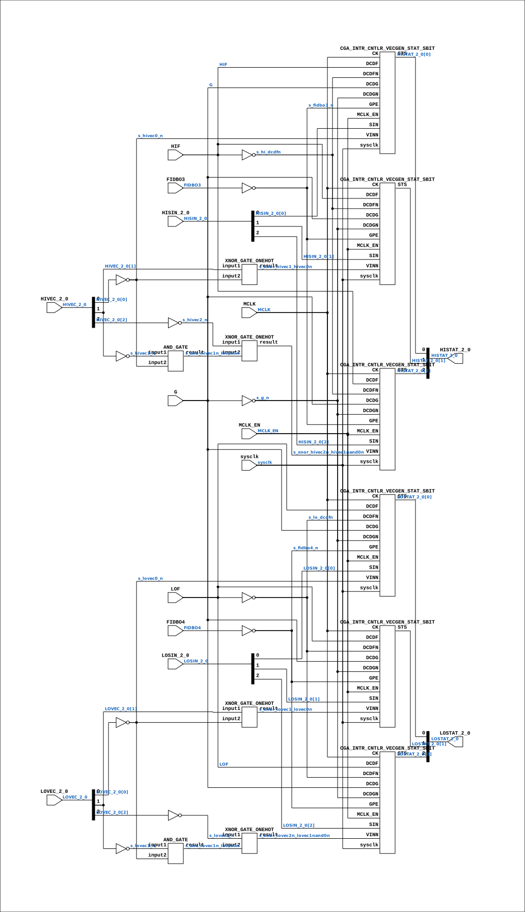
Contains: AND_GATE x2, CGA_INTR_CNTLR_VECGEN_STAT_SBIT x6, XNOR_GATE_ONEHOT x4
Module hierarchy - All modules
Schematic
Drawn from the Verilog: the yosys netlist of the Simulation (Verilator) build, instance CORE.CPU_BOARD.CPU.PROC.CGA.DELILAH.INTR.CNTLR.VECGEN.STAT. Sub-modules are boxes (click the picture to open it full size; there every sub-module box links to its page, and every wire shows its Verilog name).
Description
ND120 CGA (CPU Gate Array / DELILAH) /CGA/INTR/CNTLR/VECGEN/STAT STAT Page 87 SHEET 1 of 1 Last reviewed: 10-NOV-2024 Ronny Hansen
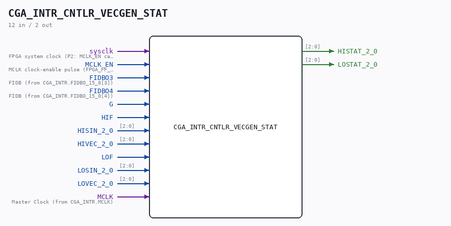
Ports
| Direction | Width | Name | Description |
|---|---|---|---|
| input | 1 |
sysclk |
FPGA system clock (P2: MCLK_EN capture) |
| input | 1 |
MCLK_EN |
MCLK clock-enable pulse (FPGA_FF_MODE, else 0) |
| input | 1 |
FIDBO3 |
FIDB (from CGA_INTR.FIDBO_15_0[3]) |
| input | 1 |
FIDBO4 |
FIDB (from CGA_INTR.FIDBO_15_0[4]) |
| input | 1 |
G |
|
| input | 1 |
HIF |
|
| input | [2:0] |
HISIN_2_0 |
|
| input | [2:0] |
HIVEC_2_0 |
|
| input | 1 |
LOF |
|
| input | [2:0] |
LOSIN_2_0 |
|
| input | [2:0] |
LOVEC_2_0 |
|
| input | 1 |
MCLK |
Master Clock (from CGA_INTR.MCLK) |
| output | [2:0] |
HISTAT_2_0 |
|
| output | [2:0] |
LOSTAT_2_0 |
Verilog source
Verilog/DELILAH-CPU/CGA_INTR/circuit/CGA_INTR_CNTLR_VECGEN_STAT.v on GitHub.
Show the Verilog of CGA_INTR_CNTLR_VECGEN_STAT (307 lines)
/**************************************************************************
** ND120 CGA (CPU Gate Array / DELILAH)                                  **
** /CGA/INTR/CNTLR/VECGEN/STAT                                           **
** STAT                                                                  **
**                                                                       **
** Page 87                                                               **
** SHEET 1 of 1                                                          **
**                                                                       **
** Last reviewed: 10-NOV-2024                                            **
** Ronny Hansen                                                          **
***************************************************************************/


module CGA_INTR_CNTLR_VECGEN_STAT (
    input       sysclk,   //! FPGA system clock (P2: MCLK_EN capture)
    input       MCLK_EN,  //! MCLK clock-enable pulse (FPGA_FF_MODE, else 0)

    input       FIDBO3,   //! FIDB (from CGA_INTR.FIDBO_15_0[3])
    input       FIDBO4,   //! FIDB (from CGA_INTR.FIDBO_15_0[4])
    input       G,
    input       HIF,
    input [2:0] HISIN_2_0,
    input [2:0] HIVEC_2_0,
    input       LOF,
    input [2:0] LOSIN_2_0,
    input [2:0] LOVEC_2_0,
    input       MCLK,     //! Master Clock (from CGA_INTR.MCLK)

    output [2:0] HISTAT_2_0,
    output [2:0] LOSTAT_2_0

);

  /*******************************************************************************
   ** The wires are defined here                                                 **
   *******************************************************************************/
  wire [2:0] s_hivec_2_0;
  wire [2:0] s_hisin_2_0;
  wire [2:0] s_losin_2_0;
  wire [2:0] s_lovec_2_0;
  wire [2:0] s_histat_2_0_out;
  wire [2:0] s_lostat_2_0_out;
  wire       s_and_hivec1n_hivec0n;
  wire       s_and_lovec1n_lovec0n;
  wire       s_fidbo3_n;
  wire       s_fidbo3;
  wire       s_fidbo4_n;
  wire       s_fidbo4;
  wire       s_g_n;
  wire       s_g;
  wire       s_hif_n;
  wire       s_hif;
  wire       s_hivec0_n;
  wire       s_hivec1_n;
  wire       s_hivec2_n;
  wire       s_lof_n;
  wire       s_lof;
  wire       s_lovec0_n;
  wire       s_lovec1_n;
  wire       s_lovec2_n;
  wire       s_mclk;
  wire       s_xnor_hivec1_hivec0n;
  wire       s_xnor_hivec2n_hivec1nand0n;
  wire       s_xnor_lovec1_lovec0n;
  wire       s_xnor_lovec2n_lovec1nand0n;

  /*******************************************************************************
   ** The module functionality is described here                                 **
   *******************************************************************************/

  /*******************************************************************************
   ** Here all input connections are defined                                     **
   *******************************************************************************/
  assign s_fidbo3         = FIDBO3;
  assign s_fidbo4         = FIDBO4;
  assign s_g              = G;
  assign s_hif            = HIF;
  assign s_hisin_2_0[2:0] = HISIN_2_0;
  assign s_hivec_2_0[2:0] = HIVEC_2_0;
  assign s_lof            = LOF;
  assign s_losin_2_0[2:0] = LOSIN_2_0;
  assign s_lovec_2_0[2:0] = LOVEC_2_0;
  assign s_mclk           = MCLK;

  /*******************************************************************************
   ** Here all output connections are defined                                    **
   *******************************************************************************/
  assign HISTAT_2_0       = s_histat_2_0_out[2:0];
  assign LOSTAT_2_0       = s_lostat_2_0_out[2:0];

  /*******************************************************************************
   ** Here all in-lined components are defined                                   **
   *******************************************************************************/

  // NOT Gate
  assign s_fidbo3_n       = ~s_fidbo3;
  assign s_fidbo4_n       = ~s_fidbo4;
  assign s_g_n            = ~s_g;
  assign s_hif_n          = ~s_hif;
  assign s_hivec0_n       = ~s_hivec_2_0[0];
  assign s_hivec1_n       = ~s_hivec_2_0[1];
  assign s_hivec2_n       = ~s_hivec_2_0[2];
  assign s_lof_n          = ~s_lof;
  assign s_lovec0_n       = ~s_lovec_2_0[0];
  assign s_lovec1_n       = ~s_lovec_2_0[1];
  assign s_lovec2_n       = ~s_lovec_2_0[2];

  /*******************************************************************************
   ** Here all normal components are defined                                     **
   *******************************************************************************/
  XNOR_GATE_ONEHOT #(
      .BubblesMask(2'b00)
  ) GATES_1 (
      .input1(s_lovec_2_0[1]),
      .input2(s_lovec0_n),
      .result(s_xnor_lovec1_lovec0n)
  );

  XNOR_GATE_ONEHOT #(
      .BubblesMask(2'b00)
  ) GATES_2 (
      .input1(s_hivec_2_0[1]),
      .input2(s_hivec0_n),
      .result(s_xnor_hivec1_hivec0n)
  );

  AND_GATE #(
      .BubblesMask(2'b11)
  ) GATES_3 (
      .input1(s_lovec1_n),
      .input2(s_lovec0_n),
      .result(s_and_lovec1n_lovec0n)
  );

  AND_GATE #(
      .BubblesMask(2'b11)
  ) GATES_4 (
      .input1(s_hivec1_n),
      .input2(s_hivec0_n),
      .result(s_and_hivec1n_hivec0n)
  );

  XNOR_GATE_ONEHOT #(
      .BubblesMask(2'b00)
  ) GATES_5 (
      .input1(s_hivec2_n),
      .input2(s_and_hivec1n_hivec0n),
      .result(s_xnor_hivec2n_hivec1nand0n)
  );

  XNOR_GATE_ONEHOT #(
      .BubblesMask(2'b00)
  ) GATES_6 (
      .input1(s_lovec2_n),
      .input2(s_and_lovec1n_lovec0n),
      .result(s_xnor_lovec2n_lovec1nand0n)
  );


  /*******************************************************************************
   ** SBIT pin mapping (see docs/RUN-level14-livelock-analysis.md)               **
   **                                                                            **
   ** The six SBIT blocks on schematic p.87 are drawn WITHOUT pin names (only    **
   ** the detail box names them), so the pin order had to be read off the        **
   ** drawing. Ronny's reads (top SBIT = HISTAT2, pins from top): pin2 = XNOR    **
   ** increment output, pin3 = HIF, pin6 = G_N.                                  **
   **                                                                            **
   ** The Am2914-correct mapping (DEFAULT) makes READ VECTOR load "vector+1"     **
   ** into the status register (the re-dispatch fence). Validated 14-JUL-2026    **
   ** in FF mode: self-test 0 STERR, RUN livelock gone (14487->1 re-dispatch),   **
   ** comparator (p.88) + IRGEL (p.90-95) audited clean, and matched against     **
   ** the C# DELILAH-L PIC ground-truth trace. Define                            **
   ** ND120_INTR_STATUS_FENCE_OFF to restore the historical dead-fence mapping.  **
   *******************************************************************************/
`ifndef ND120_INTR_STATUS_FENCE_OFF
  // Am2914 status register. Derived from the confirmed cell equation
  //   D = (SIN & DCDG & DCDF & GPE) | (DCDG & DCDFN & STS) | (VINN & DCDF & DCDGN)
  // plus the MDCD strobe polarities (G is ACTIVE LOW: G=1 idle, G=0 on
  // RDVECT/MCLR; HIF/LOF pulse on RDVECT-of-this-group and on LDSTAT):
  //   idle   : hold           (DCDG=G=1, DCDFN=HIF_n=1)
  //   LDSTAT : load S-bus     (SIN & G & HIF & group-enable)
  //   RDVECT : load vector+1  (XNOR & HIF & G_N)
  //   MCLR   : clear          (all three terms 0)
  // GPE is the group-enable bit (HIGE/LOGE, the FIDBO3/FIDBO4 buffers on the
  // sheet - otherwise unused on this page).
  wire       s_hi_dcdfn = s_hif_n;
  wire       s_hi_dcdg  = s_g;
  wire       s_hi_dcdgn = s_g_n;
  wire [2:0] s_hi_dcdf  = {3{s_hif}};
  wire [2:0] s_hi_vinn  = {s_xnor_hivec2n_hivec1nand0n, s_xnor_hivec1_hivec0n, s_hivec0_n};
  wire       s_lo_dcdfn = s_lof_n;
  wire       s_lo_dcdg  = s_g;
  wire       s_lo_dcdgn = s_g_n;
  wire [2:0] s_lo_dcdf  = {3{s_lof}};
  wire [2:0] s_lo_vinn  = {s_xnor_lovec2n_lovec1nand0n, s_xnor_lovec1_lovec0n, s_lovec0_n};
`else
  wire       s_hi_dcdfn = s_g;
  wire       s_hi_dcdg  = s_hif_n;
  wire       s_hi_dcdgn = s_fidbo3_n;
  wire [2:0] s_hi_dcdf  = {s_xnor_hivec2n_hivec1nand0n, s_xnor_hivec1_hivec0n, s_hivec0_n};
  wire [2:0] s_hi_vinn  = {3{s_g_n}};
  wire       s_lo_dcdfn = s_g;
  wire       s_lo_dcdg  = s_lof_n;
  wire       s_lo_dcdgn = s_fidbo4_n;
  wire [2:0] s_lo_dcdf  = {s_xnor_lovec2n_lovec1nand0n, s_xnor_lovec1_lovec0n, s_lovec0_n};
  wire [2:0] s_lo_vinn  = {3{s_g_n}};
`endif

`ifndef ND120_INTR_STATUS_FENCE_OFF
  wire s_hi_gpe = s_fidbo3_n;   // HIGE  (group enable, FIDBO3 buffer)
  wire s_lo_gpe = s_fidbo4_n;   // LOGE  (group enable, FIDBO4 buffer)
`else
  wire s_hi_gpe = s_hif;
  wire s_lo_gpe = s_lof;
`endif

  /*******************************************************************************
   ** Here all sub-circuits are defined                                          **
   *******************************************************************************/


  CGA_INTR_CNTLR_VECGEN_STAT_SBIT SBIT1_LO (
      .sysclk(sysclk),
      .MCLK_EN(MCLK_EN),
      .CK(s_mclk),
      .DCDF(s_lo_dcdf[1]),
      .DCDFN(s_lo_dcdfn),
      .DCDG(s_lo_dcdg),
      .DCDGN(s_lo_dcdgn),
      .GPE(s_lo_gpe),
      .SIN(s_losin_2_0[1]),
      .STS(s_lostat_2_0_out[1]),
      .VINN(s_lo_vinn[1])
  );

  CGA_INTR_CNTLR_VECGEN_STAT_SBIT SBIT2_HI (
      .sysclk(sysclk),
      .MCLK_EN(MCLK_EN),
      .CK(s_mclk),
      .DCDF(s_hi_dcdf[2]),
      .DCDFN(s_hi_dcdfn),
      .DCDG(s_hi_dcdg),
      .DCDGN(s_hi_dcdgn),
      .GPE(s_hi_gpe),
      .SIN(s_hisin_2_0[2]),
      .STS(s_histat_2_0_out[2]),
      .VINN(s_hi_vinn[2])
  );

  CGA_INTR_CNTLR_VECGEN_STAT_SBIT SBIT0_LO (
      .sysclk(sysclk),
      .MCLK_EN(MCLK_EN),
      .CK(s_mclk),
      .DCDF(s_lo_dcdf[0]),
      .DCDFN(s_lo_dcdfn),
      .DCDG(s_lo_dcdg),
      .DCDGN(s_lo_dcdgn),
      .GPE(s_lo_gpe),
      .SIN(s_losin_2_0[0]),
      .STS(s_lostat_2_0_out[0]),
      .VINN(s_lo_vinn[0])
  );

  CGA_INTR_CNTLR_VECGEN_STAT_SBIT SBIT1_HI (
      .sysclk(sysclk),
      .MCLK_EN(MCLK_EN),
      .CK(s_mclk),
      .DCDF(s_hi_dcdf[1]),
      .DCDFN(s_hi_dcdfn),
      .DCDG(s_hi_dcdg),
      .DCDGN(s_hi_dcdgn),
      .GPE(s_hi_gpe),
      .SIN(s_hisin_2_0[1]),
      .STS(s_histat_2_0_out[1]),
      .VINN(s_hi_vinn[1])
  );

  CGA_INTR_CNTLR_VECGEN_STAT_SBIT SBIT0_HI (
      .sysclk(sysclk),
      .MCLK_EN(MCLK_EN),
      .CK(s_mclk),
      .DCDF(s_hi_dcdf[0]),
      .DCDFN(s_hi_dcdfn),
      .DCDG(s_hi_dcdg),
      .DCDGN(s_hi_dcdgn),
      .GPE(s_hi_gpe),
      .SIN(s_hisin_2_0[0]),
      .STS(s_histat_2_0_out[0]),
      .VINN(s_hi_vinn[0])
  );

  CGA_INTR_CNTLR_VECGEN_STAT_SBIT SBIT2_LO (
      .sysclk(sysclk),
      .MCLK_EN(MCLK_EN),
      .CK(s_mclk),
      .DCDF(s_lo_dcdf[2]),
      .DCDFN(s_lo_dcdfn),
      .DCDG(s_lo_dcdg),
      .DCDGN(s_lo_dcdgn),
      .GPE(s_lo_gpe),
      .SIN(s_losin_2_0[2]),
      .STS(s_lostat_2_0_out[2]),
      .VINN(s_lo_vinn[2])
  );

endmodule