CGA_DCD
Source: Verilog/DELILAH-CPU/CGA_DCD/circuit/CGA_DCD.v
Where it sits (Simulation): ND120_TOP > ND120_CORE > ND3202D > CPU_15 > CPU_PROC_32 > CPU_PROC_CGA_33 > CGA > CGA_DCD
- instance path: CORE.CPU_BOARD.CPU.PROC.CGA.DELILAH.DCD
Used in: CGA (all tops)
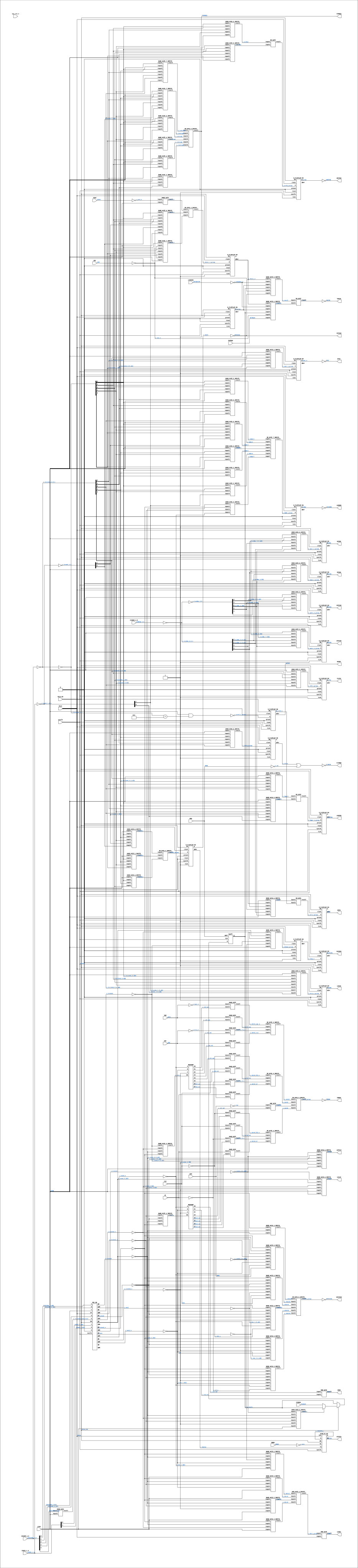
Contains: AND_GATE, D_FLIPFLOP_EN x18, NAND_GATE x14, NAND_GATE_3_INPUTS x2, NAND_GATE_4_INPUTS x9, NAND_GATE_5_INPUTS x8, NAND_GATE_6_INPUTS x19, NAND_GATE_7_INPUTS x3, NAND_GATE_8_INPUTS x8, ND38GHP x2, NOR_GATE x2, NOR_GATE_4_INPUTS, OR_GATE x4, OR_GATE_3_INPUTS x2, OR_GATE_4_INPUTS x4, OR_GATE_6_INPUTS x2, OR_GATE_7_INPUTS, R81_EN, SCAN_FF_EN
Module hierarchy - All modules
Schematic
Drawn from the Verilog: the yosys netlist of the Simulation (Verilator) build, instance CORE.CPU_BOARD.CPU.PROC.CGA.DELILAH.DCD. Sub-modules are boxes (click the picture to open it full size; there every sub-module box links to its page, and every wire shows its Verilog name).
Description
CPU GATE ARRAY - CGA - DELILAH CGA/DCD - Decoder Sheet 1-10 of 10 PDF page 65-73+75 of 108 Last reviewed: 9-FEB-2025 Ronny Hansen
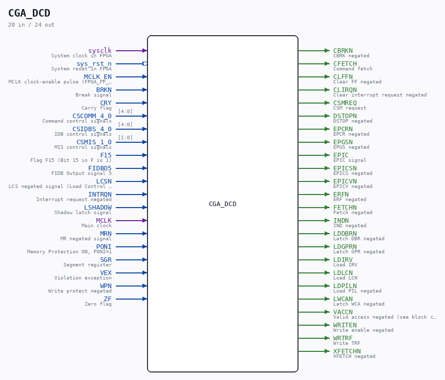
Ports
| Direction | Width | Name | Description |
|---|---|---|---|
| input | 1 |
sysclk |
System clock in FPGA |
| input | 1 |
sys_rst_n (active low) |
System reset in FPGA |
| input | 1 |
MCLK_EN |
MCLK clock-enable pulse (FPGA_FF_MODE, else 0) |
| input | 1 |
BRKN |
Break signal |
| input | 1 |
CRY |
Carry flag |
| input | [4:0] |
CSCOMM_4_0 |
Command control signals |
| input | [4:0] |
CSIDBS_4_0 |
IDB control signals |
| input | [1:0] |
CSMIS_1_0 |
MIS control signals |
| input | 1 |
F15 |
Flag F15 (Bit 15 in F is 1) |
| input | 1 |
FIDBO5 |
FIDB Output signal 5 |
| input | 1 |
LCSN |
LCS negated signal (Load Control Store) |
| input | 1 |
INTRQN |
Interrupt request negated |
| input | 1 |
LSHADOW |
Shadow latch signal |
| input | 1 |
MCLK |
Main clock |
| input | 1 |
MRN |
MR negated signal |
| input | 1 |
PONI |
Memory Protection ON, PONI=1 |
| input | 1 |
SGR |
Segment register |
| input | 1 |
VEX |
Violation exception |
| input | 1 |
WPN |
Write protect negated |
| input | 1 |
ZF |
Zero flag |
| output | 1 |
CBRKN |
CBRK negated |
| output | 1 |
CFETCH |
Command fetch |
| output | 1 |
CLFFN |
Clear FF negated |
| output | 1 |
CLIRQN |
Clear interrupt request negated |
| output | 1 |
CSMREQ |
CSM request |
| output | 1 |
DSTOPN |
DSTOP negated |
| output | 1 |
EPCRN |
EPCR negated |
| output | 1 |
EPGSN |
EPGS negated |
| output | 1 |
EPIC |
EPIC signal |
| output | 1 |
EPICSN |
EPICS negated |
| output | 1 |
EPICVN |
EPICV negated |
| output | 1 |
ERFN |
ERF negated |
| output | 1 |
FETCHN |
Fetch negated |
| output | 1 |
INDN |
IND negated |
| output | 1 |
LDDBRN |
Latch DBR negated |
| output | 1 |
LDGPRN |
Latch GPR negated |
| output | 1 |
LDIRV |
Load IRV |
| output | 1 |
LDLCN |
Load LCN |
| output | 1 |
LDPILN |
Load PIL negated |
| output | 1 |
LWCAN |
Latch WCA negated |
| output | 1 |
VACCN |
Valid access negated (see block comment, sheet 10/10) |
| output | 1 |
WRITEN |
Write enable negated |
| output | 1 |
WRTRF |
Write TRF |
| output | 1 |
XFETCHN |
XFETCH negated |
Verilog source
Verilog/DELILAH-CPU/CGA_DCD/circuit/CGA_DCD.v on GitHub.
Show the Verilog of CGA_DCD (1863 lines)
/**************************************************************************
** CPU GATE ARRAY - CGA - DELILAH **
** **
** CGA/DCD - Decoder **
** **
** Sheet 1-10 of 10 **
** PDF page 65-73+75 of 108 **
** **
** Last reviewed: 9-FEB-2025 **
** Ronny Hansen **
***************************************************************************/
module CGA_DCD (
// System input signals
input sysclk, // System clock in FPGA
input sys_rst_n, // System reset in FPGA
// Input signals
input MCLK_EN, //! MCLK clock-enable pulse (FPGA_FF_MODE, else 0)
input BRKN, //! Break signal
input CRY, //! Carry flag
input [4:0] CSCOMM_4_0, //! Command control signals
input [4:0] CSIDBS_4_0, //! IDB control signals
input [1:0] CSMIS_1_0, //! MIS control signals
input F15, //! Flag F15 (Bit 15 in F is 1)
input FIDBO5, //! FIDB Output signal 5
input LCSN, //! LCS negated signal (Load Control Store)
input INTRQN, //! Interrupt request negated
input LSHADOW, //! Shadow latch signal
input MCLK, //! Main clock
input MRN, //! MR negated signal
input PONI, //! Memory Protection ON, PONI=1
input SGR, //! Segment register
input VEX, //! Violation exception
input WPN, //! Write protect negated
input ZF, //! Zero flag
// Output signal
output CBRKN, //! CBRK negated
output CFETCH, //! Command fetch
output CLFFN, //! Clear FF negated
output CLIRQN, //! Clear interrupt request negated
output CSMREQ, //! CSM request
output DSTOPN, //! DSTOP negated
output EPCRN, //! EPCR negated
output EPGSN, //! EPGS negated
output EPIC, //! EPIC signal
output EPICSN, //! EPICS negated
output EPICVN, //! EPICV negated
output ERFN, //! ERF negated
output FETCHN, //! Fetch negated
output INDN, //! IND negated
output LDDBRN, //! Latch DBR negated
output LDGPRN, //! Latch GPR negated
output LDIRV, //! Load IRV
output LDLCN, //! Load LCN
output LDPILN, //! Load PIL negated
output LWCAN, //! Latch WCA negated
// VACCN - active-low VACC. VACC marks the cycle as a MEMORY REFERENCE THAT
// GOES THROUGH THE MMU: the page table is addressed and its status bits are
// evaluated for this access. It is the qualifier on every memory-protect
// trap term (page fault, ring violation, WIP, PGU) in CGA_TRAP, and it is
// the load enable of the PGS register in CGA_IDBCTL_PGSREG, so PGS holds
// the last logical address latched while VACC was high. Generated on sheet
// 10/10 (drawing page 75) - see the block comment at "Signal VACCN" below
// for the exact decode. Name expansion is INFERRED as "Valid ACCess"; the
// drawing gives no expansion, only the logic.
output VACCN, //! Valid access negated (see block comment, sheet 10/10)
output WRITEN, //! Write enable negated
output WRTRF, //! Write TRF
output XFETCHN //! XFETCH negated
);
/*******************************************************************************
** The wires are defined here **
*******************************************************************************/
wire [1:0] s_icsmis_1_0_n;
wire [1:0] s_icsmis_1_0;
wire [4:0] s_icscomm_4_0;
wire [4:0] s_icscomm_4_0_n;
wire [4:0] s_icsidbs_4_0;
wire [1:0] s_mis_1_0_n;
wire [1:0] s_mis_1_0;
wire [4:0] s_icsidbs_4_0_n;
wire [4:0] s_cscomm_4_0;
wire [1:0] s_csmis_1_0;
wire [4:0] s_comm_4_0;
wire [4:0] s_comm_4_0_n;
wire [4:0] s_csidbs_4_0;
wire s_brk_n;
wire s_brk;
wire s_c22_g;
wire s_c22_m0;
wire s_c22_m1;
wire s_c22_m3;
wire s_c23_m0;
wire s_c23_m1;
wire s_c23_m2;
wire s_c23_m3;
wire s_c24_g;
wire s_c24_m0;
wire s_c24_m1;
wire s_c24_m2;
wire s_c24_m3;
wire s_c25_m0;
wire s_c25_m1;
wire s_c25_m2;
wire s_c25_m3;
wire s_cbrk_group;
wire s_cbrk_n_out;
wire s_cbrk1_cry_n;
wire s_cbrk1_cry;
wire s_cbrk1_sgr_n;
wire s_cbrk1_sgr;
wire s_cbrk1;
wire s_cbrk2_f15_n;
wire s_cbrk2_f15;
wire s_cbrk2_zf_n;
wire s_cbrk2_zf;
wire s_cbrk2;
wire s_cbrk3;
wire s_cbrk4_f15_n;
wire s_cbrk4_f15;
wire s_cbrk4_zf_n;
wire s_cbrk4_zf;
wire s_cbrk4;
wire s_cfetch_out;
wire s_cfetchff_q;
wire s_clff_n_group;
wire s_clff_n_out;
wire s_clirq_n_out;
wire s_cry;
wire s_cscomm4_nand_lcsn;
wire s_csmreq_out;
wire s_csmreq1;
wire s_csmreq2;
wire s_csmreq3;
wire s_csmreq4;
wire s_csmreq5;
wire s_csmreq6;
wire s_dstop_n_out;
wire s_dstopn_group;
// DVACC chain - see the big block comment at "Signal VACCN" (sheet 10/10).
// s_dvacc1..3 are NAND outputs: each goes LOW when its condition holds, and
// each condition INHIBITS VACC. s_dvacc_n is the registered permit line and
// must be HIGH for VACC to rise.
wire s_dvacc_n; // Q-bar of MEMORY_100. High = no inhibit term active = VACC permitted this cycle.
wire s_dvacc1; // low when paging is OFF (PONI_n high) and the control store is not being loaded (LCS_n high)
wire s_dvacc2; // low on CSCOMM 0o34 or 0o35 (C4.C3.C2 = 111, C1 = 0, C0 don't-care) with CSMIS 3, no VEX, no LCS -> drawing labels 34.3, 35.3
wire s_dvacc3; // low on CSCOMM 0o37 (all five bits 1) with CSMIS 2 or 3 (CSMIS bit 0 don't-care), no LCS. No VEX input on this gate. -> labels 37.2, 37.3
wire s_emcl_n;
wire s_epcr_n_group;
wire s_epcr_n_out;
wire s_epgs_n_group;
wire s_epgs_n_out;
wire s_epic_n_group;
wire s_epic_n;
wire s_epic_out;
wire s_epics_n_group;
wire s_epics_n_out;
wire s_epicv_n_group;
wire s_epicv_n_out;
wire s_erf_n_group;
wire s_erf_n_out;
wire s_erf1;
wire s_f15;
wire s_fetch_n_out;
wire s_fetch;
wire s_fidbo5;
(* mark_debug = "true", DONT_TOUCH = "true" *) wire s_iclirq_group;
wire s_iclirq;
wire s_icomm0_n;
wire s_icomm0;
wire s_icomm1_n;
wire s_icomm1;
wire s_icomm2_n;
wire s_icomm2;
wire s_icomm4_n;
wire s_icomm4;
wire s_icry_n;
wire s_icry;
wire s_if15_n;
wire s_if15;
wire s_ifetchn_group;
wire s_ifetchn;
wire s_ifetchn1;
wire s_ifetchn2;
wire s_ifetchn3;
wire s_mis0_n;
wire s_mis0;
wire s_mis1_n;
wire s_mis1;
wire s_ind_n_out;
wire s_intrq_n;
wire s_isgr_n;
wire s_istop_n;
wire s_iwp_n;
wire s_izf_n;
wire s_izf;
wire s_lcs_n;
wire s_lddbr_group;
wire s_lddbr_n_out;
wire s_lddbr;
wire s_lddbr1;
wire s_lddbr6;
wire s_lddbr2;
wire s_lddbr3;
wire s_lddbr4;
wire s_lddbr5;
wire s_lddbr7;
wire s_ldgpr_n_group;
wire s_ldgpr_n_out;
wire s_ldgpr1;
wire s_ldgpr2;
wire s_ldirv_group;
wire s_ldirv_out;
wire s_ldirv1;
wire s_ldirv2;
wire s_ldirv3;
wire s_ldirv4;
wire s_ldlc_n_out;
wire s_ldpil_n_out;
wire s_lshadow_n;
wire s_lshadow;
wire s_lwca_n_group;
wire s_lwca_n;
wire s_mclk;
wire s_mr_n;
wire s_mr;
wire s_mreq;
wire s_poni_n;
wire s_poni;
wire s_sgr;
wire s_sioc_n;
wire s_dvacc_n_group; // D input of MEMORY_100: the three inhibit conditions OR'd together (all three OR inputs are bubbled). High = inhibit.
wire s_vacc_n_out; // ~s_vacc, driven out on the VACCN port
wire s_vacc; // VACC: this cycle is an MMU-translated memory reference (page table addressed, its status bits evaluated)
wire s_vacc1; // NAND, low when all six stage-2 terms hold with FETCH_n
wire s_vacc2; // NAND, low when all six stage-2 terms hold with INTRQ_n; OR'd with s_vacc1 through bubbled inputs
wire s_vex_n;
wire s_vex;
wire s_wp_n;
wire s_wp;
wire s_write_group;
wire s_write_n_out;
wire s_write;
wire s_write1;
wire s_write2;
wire s_wrtrf_n_group;
wire s_wrtrf_n;
wire s_wrtrf_out;
wire s_xfetch_group;
wire s_xfetch_n_out;
wire s_xfetch1;
wire s_xfetch2;
wire s_xfetch3;
wire s_xfetch4;
wire s_xfetch5;
wire s_xfetch6;
wire s_zf;
/*******************************************************************************
** Here all input connections are defined **
*******************************************************************************/
assign s_cscomm_4_0[4:0] = CSCOMM_4_0;
assign s_csmis_1_0[1:0] = CSMIS_1_0;
assign s_csidbs_4_0[4:0] = CSIDBS_4_0;
assign s_poni = PONI;
assign s_mclk = MCLK;
assign s_wp_n = WPN;
assign s_mr_n = MRN;
assign s_fidbo5 = FIDBO5;
assign s_cry = CRY;
assign s_f15 = F15;
assign s_brk_n = BRKN;
assign s_vex = VEX;
assign s_zf = ZF;
assign s_lcs_n = LCSN;
assign s_intrq_n = INTRQN;
assign s_sgr = SGR;
assign s_lshadow = LSHADOW;
// P2 (docs/plan-fix-unconstrained-clocks.md): in FF mode the MCLK-clocked
// registers capture on posedge sysclk gated by MCLK_EN (aligned to the
// MCLK rise) instead of clocking on the routed net.
`ifdef FPGA_FF_MODE
localparam MCLK_CE = 1;
`else
localparam MCLK_CE = 0;
`endif
/*******************************************************************************
** Here all output connections are defined **
*******************************************************************************/
assign CBRKN = s_cbrk_n_out;
assign CFETCH = s_cfetch_out;
assign CLFFN = s_clff_n_out;
assign CLIRQN = s_clirq_n_out;
assign CSMREQ = s_csmreq_out;
assign DSTOPN = s_dstop_n_out;
assign EPCRN = s_epcr_n_out;
assign EPGSN = s_epgs_n_out;
assign EPIC = s_epic_out;
assign EPICSN = s_epics_n_out;
assign EPICVN = s_epicv_n_out;
assign ERFN = s_erf_n_out;
assign FETCHN = s_fetch_n_out;
assign INDN = s_ind_n_out;
assign LDDBRN = s_lddbr_n_out;
assign LDGPRN = s_ldgpr_n_out;
assign LDIRV = s_ldirv_out;
assign LDLCN = s_ldlc_n_out;
assign LDPILN = s_ldpil_n_out;
assign LWCAN = s_lwca_n;
assign VACCN = s_vacc_n_out;
assign WRITEN = s_write_n_out;
assign WRTRF = s_wrtrf_out;
assign XFETCHN = s_xfetch_n_out;
/*******************************************************************************
** Here all in-lined components are defined **
*******************************************************************************/
// NOT Gate
assign s_comm_4_0_n[0] = ~s_icomm0;
assign s_comm_4_0_n[1] = ~s_icomm1;
assign s_comm_4_0_n[2] = ~s_icomm2;
assign s_comm_4_0_n[3] = ~s_comm_4_0[3];
assign s_comm_4_0_n[4] = ~s_icomm4;
assign s_comm_4_0[0] = ~s_icomm0_n;
assign s_comm_4_0[1] = ~s_icomm1_n;
assign s_comm_4_0[2] = ~s_icomm2_n;
assign s_comm_4_0[4] = ~s_icomm4_n;
assign s_mis_1_0_n[0] = ~s_mis0;
assign s_mis_1_0_n[1] = ~s_mis1;
assign s_mis_1_0[0] = ~s_mis0_n;
assign s_mis_1_0[1] = ~s_mis1_n;
assign s_vacc_n_out = ~s_vacc;
assign s_xfetch_n_out = ~s_xfetch_group;
assign s_brk = ~s_brk_n;
assign s_cbrk_n_out = ~s_cbrk_group;
assign s_epic_out = ~s_epic_n;
assign s_fetch_n_out = ~s_fetch;
assign s_icry = ~s_icry_n;
assign s_icry_n = ~s_cry;
assign s_if15 = ~s_if15_n;
assign s_if15_n = ~s_f15;
assign s_isgr_n = ~s_sgr;
assign s_iwp_n = ~s_wp;
assign s_izf = ~s_izf_n;
assign s_izf_n = ~s_zf;
assign s_lddbr_n_out = ~s_lddbr;
assign s_lshadow_n = ~s_lshadow;
assign s_mr = ~s_mr_n;
assign s_poni_n = ~s_poni;
assign s_vex_n = ~s_vex;
assign s_wp = ~s_wp_n;
assign s_write_n_out = ~s_write;
/*******************************************************************************
** Here all normal components are defined **
*******************************************************************************/
/* Sheet 1/10 - page 65 */
/* BUFFERING CSCOMM to ICSCOMM */
assign s_icscomm_4_0_n[4:0] = ~s_cscomm_4_0[4:0]; // Buffered (intern) negated cscomm
assign s_icscomm_4_0[4:0] = ~s_icscomm_4_0_n[4:0]; // Buffered (intern) double negated cscomm
/* Sheet 1/10 - page 65 */
/* BUFFERING CSMIS to ICSMIS */
assign s_icsmis_1_0_n[1:0] = ~s_csmis_1_0[1:0]; // Buffered (intern) negated csmis
assign s_icsmis_1_0[1:0] = ~s_icsmis_1_0_n[1:0]; // Buffered (intern) double negated csmis
/* Sheet 8/10 - page 72 */
/* BUFFERING CSMIS to ICSMIS */
assign s_icsidbs_4_0_n[4:0] = ~s_csidbs_4_0[4:0]; // Buffered (intern) negated csidbs
assign s_icsidbs_4_0[4:0] = ~s_icsidbs_4_0_n[4:0]; // Buffered (intern) double negated csidbs
/* Sheet 1/10 - page 65 */
/* LATCHING CSCOMM to COMM */
/* LATCHING CSMIS to MIS */
NAND_GATE #(
.BubblesMask(2'b00)
) GATES_60 (
.input1(s_cscomm_4_0[4]),
.input2(s_lcs_n),
.result(s_cscomm4_nand_lcsn)
);
// P2: domain MCLK (posedge s_mclk) -> MCLK_EN
R81_EN #(.USE_ENABLE(MCLK_CE)) COMM_MIS_REG (
.sysclk(sysclk),
.EN(MCLK_EN),
.CP(s_mclk),
.A(s_cscomm_4_0[0]),
.B(s_cscomm_4_0[1]),
.C(s_cscomm_4_0[2]),
.D(s_cscomm_4_0[3]),
.E(s_cscomm4_nand_lcsn),
.F(s_csmis_1_0[0]),
.G(s_csmis_1_0[1]),
.H(1'b0),
.QA (s_icomm0),
.QAN(s_icomm0_n),
.QB (s_icomm1),
.QBN(s_icomm1_n),
.QC (s_icomm2),
.QCN(s_icomm2_n),
.QD (s_comm_4_0[3]),
.QDN(),
.QE (s_icomm4_n),
.QEN(s_icomm4),
.QF (s_mis0),
.QFN(s_mis0_n),
.QG (s_mis1),
.QGN(s_mis1_n),
.QH (),
.QHN()
);
/************************************************************************************************************/
/* Sheet 2/10 - page 66 */
/* Signal XFETCHN */
NAND_GATE_3_INPUTS #(
.BubblesMask(3'b000)
) GATES_63 (
.input1(s_comm_4_0[4]),
.input2(s_comm_4_0_n[3]),
.input3(s_comm_4_0[2]),
.result(s_xfetch1)
);
NAND_GATE_8_INPUTS #(
.BubblesMask(8'h00)
) GATES_72 (
.input1(s_comm_4_0[4]),
.input2(s_comm_4_0_n[3]),
.input3(s_comm_4_0_n[2]),
.input4(s_comm_4_0[1]),
.input5(s_comm_4_0_n[0]),
.input6(s_mis_1_0[1]),
.input7(s_mis_1_0[0]),
.input8(s_iwp_n),
.result(s_xfetch2)
);
NAND_GATE_8_INPUTS #(
.BubblesMask(8'h00)
) GATES_80 (
.input1(s_comm_4_0[4]),
.input2(s_comm_4_0_n[3]),
.input3(s_comm_4_0_n[2]),
.input4(s_comm_4_0[1]),
.input5(s_comm_4_0[0]),
.input6(s_mis_1_0_n[1]),
.input7(s_mis_1_0_n[0]),
.input8(s_if15),
.result(s_xfetch3)
);
NAND_GATE_8_INPUTS #(
.BubblesMask(8'h00)
) GATES_7 (
.input1(s_comm_4_0[4]),
.input2(s_comm_4_0_n[3]),
.input3(s_comm_4_0_n[2]),
.input4(s_comm_4_0[1]),
.input5(s_comm_4_0[0]),
.input6(s_mis_1_0_n[1]),
.input7(s_mis_1_0[0]),
.input8(s_if15_n),
.result(s_xfetch4)
);
NAND_GATE_8_INPUTS #(
.BubblesMask(8'h00)
) GATES_11 (
.input1(s_comm_4_0[4]),
.input2(s_comm_4_0_n[3]),
.input3(s_comm_4_0_n[2]),
.input4(s_comm_4_0[1]),
.input5(s_comm_4_0[0]),
.input6(s_mis_1_0[1]),
.input7(s_izf),
.input8(s_mis_1_0_n[0]),
.result(s_xfetch5)
);
NAND_GATE_8_INPUTS #(
.BubblesMask(8'h00)
) GATES_12 (
.input1(s_comm_4_0[4]),
.input2(s_comm_4_0_n[3]),
.input3(s_comm_4_0_n[2]),
.input4(s_comm_4_0[1]),
.input5(s_comm_4_0[0]),
.input6(s_mis_1_0[1]),
.input7(s_mis_1_0[0]),
.input8(s_izf_n),
.result(s_xfetch6)
);
OR_GATE_6_INPUTS #(
.BubblesMask({2'b11, 4'hF})
) GATES_4 (
.input1(s_xfetch1),
.input2(s_xfetch2),
.input3(s_xfetch3),
.input4(s_xfetch4),
.input5(s_xfetch5),
.input6(s_xfetch6),
.result(s_xfetch_group)
);
/************************************************************************************************************/
//** IALUR ? **/
/************************************************************************************************************/
/* Sheet 3/10 - page 67 */
/*** Signalk IND_n ****/
/*** Input: COMM ***/
// Gate enable
NAND_GATE_4_INPUTS #(
.BubblesMask(4'h0)
) GATES_16 (
.input1(s_comm_4_0[1]),
.input2(s_comm_4_0_n[2]),
.input3(s_comm_4_0_n[3]),
.input4(s_comm_4_0[4]),
.result(s_c22_g)
);
ND38GHP C22 (
.A(s_mis_1_0[0]),
.B(s_mis_1_0[1]),
.C(s_comm_4_0[0]),
.GN(s_c22_g),
.Z0(s_c22_m0),
.Z1(s_c22_m1),
.Z2(),
.Z3(s_c22_m3),
.Z4(s_c23_m0),
.Z5(s_c23_m1),
.Z6(s_c23_m2),
.Z7(s_c23_m3)
);
NOR_GATE #(
.BubblesMask(2'b00)
) GATES_20 (
.input1(s_c22_m0),
.input2(s_c22_m1),
.result(s_ind_n_out)
);
/*** Signal CBRKN ****/
/*** Input: COMM ***/
// Gate enable for input to CBRKN
NAND_GATE_4_INPUTS #(
.BubblesMask(4'h0)
) GATES_39 (
.input1(s_comm_4_0_n[1]),
.input2(s_comm_4_0[2]),
.input3(s_comm_4_0_n[3]),
.input4(s_comm_4_0[4]),
.result(s_c24_g)
);
ND38GHP C24 (
.A(s_mis_1_0[0]),
.B(s_mis_1_0[1]),
.C(s_comm_4_0[0]),
.GN(s_c24_g),
.Z0(s_c24_m0),
.Z1(s_c24_m1),
.Z2(s_c24_m2),
.Z3(s_c24_m3),
.Z4(s_c25_m0),
.Z5(s_c25_m1),
.Z6(s_c25_m2),
.Z7(s_c25_m3)
);
NAND_GATE #(
.BubblesMask(2'b00)
) GATES_40 (
.input1(s_isgr_n),
.input2(s_c24_m0),
.result(s_cbrk1_sgr_n)
);
NAND_GATE #(
.BubblesMask(2'b00)
) GATES_41 (
.input1(s_sgr),
.input2(s_c24_m1),
.result(s_cbrk1_sgr)
);
NAND_GATE #(
.BubblesMask(2'b00)
) GATES_42 (
.input1(s_icry_n),
.input2(s_c24_m2),
.result(s_cbrk1_cry_n)
);
NAND_GATE #(
.BubblesMask(2'b00)
) GATES_43 (
.input1(s_icry),
.input2(s_c24_m3),
.result(s_cbrk1_cry)
);
OR_GATE_4_INPUTS #(
.BubblesMask(4'hF)
) GATES_44 (
.input1(s_cbrk1_sgr_n),
.input2(s_cbrk1_sgr),
.input3(s_cbrk1_cry_n),
.input4(s_cbrk1_cry),
.result(s_cbrk1)
);
NAND_GATE #(
.BubblesMask(2'b00)
) GATES_48 (
.input1(s_if15_n),
.input2(s_c25_m0),
.result(s_cbrk2_f15_n)
);
NAND_GATE #(
.BubblesMask(2'b00)
) GATES_49 (
.input1(s_if15),
.input2(s_c25_m1),
.result(s_cbrk2_f15)
);
NAND_GATE #(
.BubblesMask(2'b00)
) GATES_50 (
.input1(s_izf_n),
.input2(s_c25_m2),
.result(s_cbrk2_zf_n)
);
NAND_GATE #(
.BubblesMask(2'b00)
) GATES_52 (
.input1(s_izf),
.input2(s_c25_m3),
.result(s_cbrk2_zf)
);
OR_GATE_4_INPUTS #(
.BubblesMask(4'hF)
) GATES_53 (
.input1(s_cbrk2_f15_n),
.input2(s_cbrk2_f15),
.input3(s_cbrk2_zf_n),
.input4(s_cbrk2_zf),
.result(s_cbrk2)
);
AND_GATE #(
.BubblesMask(2'b00)
) GATES_24 (
.input1(s_wp),
.input2(s_c22_m3),
.result(s_cbrk3)
);
NAND_GATE #(
.BubblesMask(2'b00)
) GATES_25 (
.input1(s_if15_n),
.input2(s_c23_m0),
.result(s_cbrk4_f15_n)
);
NAND_GATE #(
.BubblesMask(2'b00)
) GATES_28 (
.input1(s_if15),
.input2(s_c23_m1),
.result(s_cbrk4_f15)
);
NAND_GATE #(
.BubblesMask(2'b00)
) GATES_31 (
.input1(s_izf_n),
.input2(s_c23_m2),
.result(s_cbrk4_zf_n)
);
NAND_GATE #(
.BubblesMask(2'b00)
) GATES_33 (
.input1(s_izf),
.input2(s_c23_m3),
.result(s_cbrk4_zf)
);
OR_GATE_4_INPUTS #(
.BubblesMask(4'hF)
) GATES_34 (
.input1(s_cbrk4_f15_n),
.input2(s_cbrk4_f15),
.input3(s_cbrk4_zf_n),
.input4(s_cbrk4_zf),
.result(s_cbrk4)
);
OR_GATE_4_INPUTS #(
.BubblesMask(4'h0)
) GATES_54 (
.input1(s_cbrk1),
.input2(s_cbrk2),
.input3(s_cbrk3),
.input4(s_cbrk4),
.result(s_cbrk_group)
);
/************************************************************************************************************/
/* Sheet 4/10 - page 68 */
/*** Signal LDLCN ****/
/*** Input: COMM ***/
NAND_GATE_6_INPUTS #(
.BubblesMask({2'b00, 4'h0})
) GATES_65 (
.input1(s_comm_4_0_n[4]),
.input2(s_comm_4_0[3]),
.input3(s_comm_4_0[2]),
.input4(s_comm_4_0[1]),
.input5(s_comm_4_0[0]),
.input6(s_lcs_n),
.result(s_ldlc_n_out)
);
/*** Signal LDIRV ****/
/*** Input: COMM ***/
NAND_GATE_6_INPUTS #(
.BubblesMask({2'b00, 4'h0})
) GATES_79 (
.input1(s_comm_4_0[4]),
.input2(s_comm_4_0_n[3]),
.input3(s_comm_4_0_n[0]),
.input4(s_mis_1_0[1]),
.input5(s_mis_1_0[0]),
.input6(s_lcs_n),
.result(s_ldirv1)
);
NAND_GATE_5_INPUTS #(
.BubblesMask({1'b0, 4'h0})
) GATES_3 (
.input1(s_comm_4_0[4]),
.input2(s_comm_4_0_n[3]),
.input3(s_comm_4_0[1]),
.input4(s_mis_1_0[1]),
.input5(s_lcs_n),
.result(s_ldirv2)
);
NAND_GATE_5_INPUTS #(
.BubblesMask({1'b0, 4'h0})
) GATES_8 (
.input1(s_comm_4_0[4]),
.input2(s_comm_4_0_n[3]),
.input3(s_comm_4_0[1]),
.input4(s_comm_4_0[0]),
.input5(s_lcs_n),
.result(s_ldirv3)
);
NAND_GATE_4_INPUTS #(
.BubblesMask(4'h0)
) GATES_9 (
.input1(s_comm_4_0[4]),
.input2(s_comm_4_0_n[3]),
.input3(s_comm_4_0[2]),
.input4(s_lcs_n),
.result(s_ldirv4)
);
NOR_GATE_4_INPUTS #(
.BubblesMask(4'hF)
) GATES_6 (
.input1(s_ldirv1),
.input2(s_ldirv2),
.input3(s_ldirv3),
.input4(s_ldirv4),
.result(s_ldirv_group)
);
NOR_GATE #(
.BubblesMask(2'b00)
) GATES_10 (
.input1(s_ldirv_group),
.input2(s_mclk),
.result(s_ldirv_out)
);
/*** Signal LDPILN ****/
/*** Input: COMM ***/
NAND_GATE_6_INPUTS #(
.BubblesMask({2'b00, 4'h0})
) GATES_13 (
.input1(s_comm_4_0_n[4]),
.input2(s_comm_4_0_n[3]),
.input3(s_comm_4_0_n[2]),
.input4(s_comm_4_0_n[1]),
.input5(s_comm_4_0[0]),
.input6(s_lcs_n),
.result(s_ldpil_n_out)
);
/*** Signal SIOCN ****/
/*** Input: COMM ***/
NAND_GATE_6_INPUTS #(
.BubblesMask({2'b00, 4'h0})
) GATES_15 (
.input1(s_comm_4_0_n[4]),
.input2(s_comm_4_0_n[3]),
.input3(s_comm_4_0[2]),
.input4(s_comm_4_0[1]),
.input5(s_comm_4_0[0]),
.input6(s_lcs_n),
.result(s_sioc_n)
);
/************************************************************************************************************/
/* Sheet 5/10 - page 69 */
/*** Signal LDDBRN ****/
/*** Input: ICSCOMM ***/
NAND_GATE_5_INPUTS #(
.BubblesMask({1'b0, 4'h0})
) GATES_18 (
.input1(s_icscomm_4_0[4]),
.input2(s_icscomm_4_0[3]),
.input3(s_icscomm_4_0_n[2]),
.input4(s_icscomm_4_0_n[1]),
.input5(s_lcs_n),
.result(s_lddbr1)
);
NAND_GATE_5_INPUTS #(
.BubblesMask({1'b0, 4'h0})
) GATES_19 (
.input1(s_icscomm_4_0[4]),
.input2(s_icscomm_4_0[3]),
.input3(s_icscomm_4_0_n[1]),
.input4(s_icscomm_4_0_n[0]),
.input5(s_lcs_n),
.result(s_lddbr2)
);
NAND_GATE_6_INPUTS #(
.BubblesMask({2'b00, 4'h0})
) GATES_21 (
.input1(s_icscomm_4_0[4]),
.input2(s_icscomm_4_0[2]),
.input3(s_icscomm_4_0[1]),
.input4(s_icscomm_4_0[0]),
.input5(s_icsmis_1_0[1]),
.input6(s_lcs_n),
.result(s_lddbr3)
);
NAND_GATE_5_INPUTS #(
.BubblesMask({1'b0, 4'h0})
) GATES_22 (
.input1(s_icscomm_4_0[4]),
.input2(s_icscomm_4_0_n[3]),
.input3(s_icscomm_4_0[1]),
.input4(s_icscomm_4_0[0]),
.input5(s_lcs_n),
.result(s_lddbr4)
);
NAND_GATE_3_INPUTS #(
.BubblesMask(3'b000)
) GATES_26 (
.input1(s_icscomm_4_0[4]),
.input2(s_icscomm_4_0_n[3]),
.input3(s_icscomm_4_0[2]),
.result(s_lddbr5)
);
NAND_GATE_4_INPUTS #(
.BubblesMask(4'h0)
) GATES_29 (
.input1(s_icscomm_4_0[4]),
.input2(s_icscomm_4_0_n[3]),
.input3(s_icscomm_4_0[1]),
.input4(s_icsmis_1_0_n[1]),
.result(s_lddbr6)
);
NAND_GATE_4_INPUTS #(
.BubblesMask(4'h0)
) GATES_32 (
.input1(s_comm_4_0[4]),
.input2(s_comm_4_0_n[3]),
.input3(s_comm_4_0[1]),
.input4(s_mis_1_0[0]),
.result(s_lddbr7)
);
OR_GATE_7_INPUTS #(
.BubblesMask({3'b111, 4'hF})
) GATES_23 (
.input1(s_lddbr1),
.input2(s_lddbr2),
.input3(s_lddbr3),
.input4(s_lddbr4),
.input5(s_lddbr5),
.input6(s_lddbr6),
.input7(s_lddbr7),
.result(s_lddbr_group)
);
// P2: domain MCLK (posedge s_mclk) -> MCLK_EN
D_FLIPFLOP_EN #(
.USE_ENABLE(MCLK_CE)
) MEMORY_88 (
.sysclk(sysclk),
.EN(MCLK_EN),
.clock(s_mclk),
.d(s_lddbr_group),
.preset(1'b0),
.q(s_lddbr),
.qBar(),
.reset(1'b0),
.tick(1'b1)
);
/*** Signal FETCHN ****/
/*** Input: ICSCOMM ***/
NAND_GATE_6_INPUTS #(
.BubblesMask({2'b00, 4'h0})
) GATES_35 (
.input1(s_lcs_n),
.input2(s_icscomm_4_0[4]),
.input3(s_icscomm_4_0_n[3]),
.input4(s_icscomm_4_0[1]),
.input5(s_icsmis_1_0[1]),
.input6(s_icsmis_1_0[0]),
.result(s_ifetchn1)
);
NAND_GATE_5_INPUTS #(
.BubblesMask({1'b0, 4'h0})
) GATES_36 (
.input1(s_lcs_n),
.input2(s_icscomm_4_0[4]),
.input3(s_icscomm_4_0_n[3]),
.input4(s_icscomm_4_0[1]),
.input5(s_icscomm_4_0[0]),
.result(s_ifetchn2)
);
NAND_GATE_4_INPUTS #(
.BubblesMask(4'h0)
) GATES_38 (
.input1(s_lcs_n),
.input2(s_icscomm_4_0[4]),
.input3(s_icscomm_4_0_n[3]),
.input4(s_icscomm_4_0[2]),
.result(s_ifetchn3)
);
OR_GATE_3_INPUTS #(
.BubblesMask(3'b111)
) GATES_37 (
.input1(s_ifetchn1),
.input2(s_ifetchn2),
.input3(s_ifetchn3),
.result(s_ifetchn_group)
);
// P2: domain MCLK (posedge s_mclk) -> MCLK_EN
D_FLIPFLOP_EN #(
.USE_ENABLE(MCLK_CE)
) MEMORY_90 (
.sysclk(sysclk),
.EN(MCLK_EN),
.clock(s_mclk),
.d(s_ifetchn_group),
.preset(1'b0),
.q(s_fetch),
.qBar(s_ifetchn),
.reset(1'b0),
.tick(1'b1)
);
/*** Signal CFETCHN ****/
/*** Input: ICSCOMM ***/
// P2: domain MCLK (posedge s_mclk) -> MCLK_EN
SCAN_FF_EN #(.USE_ENABLE(MCLK_CE)) CFETCH_FF (
.sysclk(sysclk),
.EN(MCLK_EN),
.CLK(s_mclk),
.D (s_cfetchff_q),
.TE (s_brk),
.TI (s_ifetchn),
.Q (s_cfetchff_q),
.QN (s_cfetch_out)
);
/************************************************************************************************************/
/* Sheet 6/10 - page 70 */
/*** Signal WRITEN ****/
/*** Input: ICSCOMM ***/
NAND_GATE_5_INPUTS #(
.BubblesMask({1'b0, 4'h0})
) GATES_45 (
.input1(s_icscomm_4_0[4]),
.input2(s_icscomm_4_0[3]),
.input3(s_icscomm_4_0_n[2]),
.input4(s_icscomm_4_0[1]),
.input5(s_lcs_n),
.result(s_write1) //command 32,33
);
NAND_GATE_6_INPUTS #(
.BubblesMask({2'b00, 4'h0})
) GATES_47 (
.input1(s_icscomm_4_0[4]),
.input2(s_icscomm_4_0[3]),
.input3(s_icscomm_4_0[2]),
.input4(s_icscomm_4_0_n[1]),
.input5(s_icscomm_4_0[0]),
.input6(s_lcs_n),
.result(s_write2) //command 35
);
OR_GATE #(
.BubblesMask(2'b11)
) GATES_46 (
.input1(s_write1),
.input2(s_write2),
.result(s_write_group)
);
// P2: domain MCLK (posedge s_mclk) -> MCLK_EN
D_FLIPFLOP_EN #(
.USE_ENABLE(MCLK_CE)
) MEMORY_91 (
.sysclk(sysclk),
.EN(MCLK_EN),
.clock(s_mclk),
.d(s_write_group),
.preset(1'b0),
.q(s_write),
.qBar(),
.reset(1'b0),
.tick(1'b1)
);
/*** Signal CLFFN ****/
/*** Input: ICSCOMM ***/
NAND_GATE_6_INPUTS #(
.BubblesMask({2'b00, 4'h0})
) GATES_51 (
.input1(s_lcs_n),
.input2(s_icscomm_4_0_n[4]),
.input3(s_icscomm_4_0[3]),
.input4(s_icscomm_4_0[2]),
.input5(s_icscomm_4_0[1]),
.input6(s_icscomm_4_0_n[0]),
.result(s_clff_n_group) //16
);
// P2: domain MCLK (posedge s_mclk) -> MCLK_EN
D_FLIPFLOP_EN #(
.USE_ENABLE(MCLK_CE)
) MEMORY_92 (
.sysclk(sysclk),
.EN(MCLK_EN),
.clock(s_mclk),
.d(s_clff_n_group),
.preset(1'b0),
.q(s_clff_n_out),
.qBar(),
.reset(1'b0),
.tick(1'b1)
);
/*** Signal CLIRQN ****/
/*** Input: ICSCOMM ***/
NAND_GATE_6_INPUTS #(
.BubblesMask({2'b00, 4'h0})
) GATES_55 (
.input1(s_lcs_n),
.input2(s_icscomm_4_0_n[4]),
.input3(s_icscomm_4_0_n[3]),
.input4(s_icscomm_4_0[2]),
.input5(s_icscomm_4_0_n[1]),
.input6(s_icscomm_4_0_n[0]),
.result(s_iclirq_group) //04
);
// P2: domain MCLK (posedge s_mclk) -> MCLK_EN
D_FLIPFLOP_EN #(
.USE_ENABLE(MCLK_CE)
) MEMORY_93 (
.sysclk(sysclk),
.EN(MCLK_EN),
.clock(s_mclk),
.d(s_iclirq_group),
.preset(1'b0),
.q(),
.qBar(s_iclirq),
.reset(1'b0),
.tick(1'b1)
);
/*
NOR_GATE #(.BubblesMask(2'b00))
GATES_56 (.input1(s_iclirq),
.input2(s_mr),
.result(s_clirq_n_out));
*/
assign s_clirq_n_out = ~(s_iclirq | s_mr);
/*** Signal EPIC ****/
/*** Input: ICSCOMM ***/
NAND_GATE_6_INPUTS #(
.BubblesMask({2'b00, 4'h0})
) GATES_57 (
.input1(s_lcs_n),
.input2(s_icscomm_4_0_n[4]),
.input3(s_icscomm_4_0[3]),
.input4(s_icscomm_4_0_n[2]),
.input5(s_icscomm_4_0_n[1]),
.input6(s_icscomm_4_0[0]),
.result(s_epic_n_group)
);
// P2: domain MCLK (posedge s_mclk) -> MCLK_EN
D_FLIPFLOP_EN #(
.USE_ENABLE(MCLK_CE)
) MEMORY_94 (
.sysclk(sysclk),
.EN(MCLK_EN),
.clock(s_mclk),
.d(s_epic_n_group),
.preset(1'b0),
.q(s_epic_n),
.qBar(),
.reset(1'b0),
.tick(1'b1)
);
/************************************************************************************************************/
/* Sheet 7/10 - page 71 */
/*** Signal LWCAN ****/
/*** Input: ICSCOMM ***/
NAND_GATE_8_INPUTS #(
.BubblesMask(8'h00)
) GATES_58 (
.input1(s_lcs_n),
.input2(s_icscomm_4_0[4]),
.input3(s_icscomm_4_0[3]),
.input4(s_icscomm_4_0[2]),
.input5(s_icscomm_4_0[1]),
.input6(s_icscomm_4_0_n[0]),
.input7(s_icsmis_1_0_n[1]),
.input8(s_icsmis_1_0_n[0]),
.result(s_lwca_n_group)
);
// P2: domain MCLK (posedge s_mclk) -> MCLK_EN
D_FLIPFLOP_EN #(
.USE_ENABLE(MCLK_CE)
) MEMORY_95 (
.sysclk(sysclk),
.EN(MCLK_EN),
.clock(s_mclk),
.d(s_lwca_n_group),
.preset(1'b0),
.q(s_lwca_n),
.qBar(),
.reset(1'b0),
.tick(1'b1)
);
/*** Signal LDGPRN ****/
/*** Input: ICSCOMM ***/
NAND_GATE_6_INPUTS #(
.BubblesMask({2'b00, 4'h0})
) GATES_61 (
.input1(s_lcs_n),
.input2(s_icscomm_4_0_n[4]),
.input3(s_icscomm_4_0_n[3]),
.input4(s_icscomm_4_0_n[2]),
.input5(s_icscomm_4_0[1]),
.input6(s_icscomm_4_0_n[0]),
.result(s_ldgpr1) // 2.n
);
NAND_GATE_8_INPUTS #(
.BubblesMask(8'h00)
) GATES_64 (
.input1(s_lcs_n),
.input2(s_icscomm_4_0[4]),
.input3(s_icscomm_4_0_n[3]),
.input4(s_icscomm_4_0_n[2]),
.input5(s_icscomm_4_0[1]),
.input6(s_icscomm_4_0_n[0]),
.input7(s_icsmis_1_0[1]),
.input8(s_icsmis_1_0_n[0]),
.result(s_ldgpr2) //22.2
);
OR_GATE #(
.BubblesMask(2'b11)
) GATES_62 (
.input1(s_ldgpr1),
.input2(s_ldgpr2),
.result(s_ldgpr_n_group)
);
// P2: domain MCLK (posedge s_mclk) -> MCLK_EN
D_FLIPFLOP_EN #(
.USE_ENABLE(MCLK_CE)
) MEMORY_96 (
.sysclk(sysclk),
.EN(MCLK_EN),
.clock(s_mclk),
.d(s_ldgpr_n_group),
.preset(1'b0),
.q(),
.qBar(s_ldgpr_n_out),
.reset(1'b0),
.tick(1'b1)
);
/*** Signal WRTRF / WRTRFN ****/
/*** Input: ICSCOMM ***/
assign s_wrtrf_n_group = ~(s_lcs_n & (s_icscomm_4_0 == 5'b00011));
/*
NAND_GATE_6_INPUTS #(
.BubblesMask({2'b00, 4'h0})
) GATES_66 (
.input1(s_lcs_n),
.input2(s_icscomm_4_0_n[4]),
.input3(s_icscomm_4_0_n[3]),
.input4(s_icscomm_4_0_n[2]),
.input5(s_icscomm_4_0[1]),
.input6(s_icscomm_4_0[0]),
.result(s_wrtrf_n_group)
);
*/
// P2: domain MCLK (posedge s_mclk) -> MCLK_EN
D_FLIPFLOP_EN #(
.USE_ENABLE(MCLK_CE)
) MEMORY_98 (
.sysclk(sysclk),
.EN(MCLK_EN),
.clock(s_mclk),
.d(s_wrtrf_n_group),
.preset(1'b0),
.q(s_wrtrf_n),
.qBar(s_wrtrf_out),
.reset(1'b0),
.tick(1'b1)
);
/************************************************************************************************************/
/* Sheet 8/10 - page 72 */
/* Enable IDB sources */
/*** Signal EPGSN (Enable PGS negated - to IDB bus)****/
/*** Input: ICSIDBS ***/
NAND_GATE_6_INPUTS #(
.BubblesMask({2'b00, 4'h0})
) GATES_59 (
.input1(s_lcs_n),
.input2(s_icsidbs_4_0[4]),
.input3(s_icsidbs_4_0_n[3]),
.input4(s_icsidbs_4_0_n[2]),
.input5(s_icsidbs_4_0[1]),
.input6(s_icsidbs_4_0[0]),
.result(s_epgs_n_group)
);
// P2: domain MCLK (posedge s_mclk) -> MCLK_EN
D_FLIPFLOP_EN #(
.USE_ENABLE(MCLK_CE)
) MEMORY_97 (
.sysclk(sysclk),
.EN(MCLK_EN),
.clock(s_mclk),
.d(s_epgs_n_group),
.preset(1'b0),
.q(s_epgs_n_out),
.qBar(),
.reset(1'b0),
.tick(1'b1)
);
/*** Signal EPRCN (Enable PCR Negated - to IDB bus) ****/
/*** Input: ICSIDBS ***/
NAND_GATE_6_INPUTS #(
.BubblesMask({2'b00, 4'h0})
) GATES_5 (
.input1(s_lcs_n),
.input2(s_icsidbs_4_0[4]),
.input3(s_icsidbs_4_0_n[3]),
.input4(s_icsidbs_4_0[2]),
.input5(s_icsidbs_4_0_n[1]),
.input6(s_icsidbs_4_0[0]),
.result(s_epcr_n_group)
);
// P2: domain MCLK (posedge s_mclk) -> MCLK_EN
D_FLIPFLOP_EN #(
.USE_ENABLE(MCLK_CE)
) MEMORY_85 (
.sysclk(sysclk),
.EN(MCLK_EN),
.clock(s_mclk),
.d(s_epcr_n_group),
.preset(1'b0),
.q(s_epcr_n_out),
.qBar(),
.reset(1'b0),
.tick(1'b1)
);
/*** Signal EPICVN (Enable PICV negated - to IDB bus) ****/
/*** Input: ICSIDBS ***/
NAND_GATE_6_INPUTS #(
.BubblesMask({2'b00, 4'h0})
) GATES_14 (
.input1(s_lcs_n),
.input2(s_icsidbs_4_0[4]),
.input3(s_icsidbs_4_0[3]),
.input4(s_icsidbs_4_0_n[2]),
.input5(s_icsidbs_4_0_n[1]),
.input6(s_icsidbs_4_0[0]),
.result(s_epicv_n_group)
);
// P2: domain MCLK (posedge s_mclk) -> MCLK_EN
D_FLIPFLOP_EN #(
.USE_ENABLE(MCLK_CE)
) MEMORY_86 (
.sysclk(sysclk),
.EN(MCLK_EN),
.clock(s_mclk),
.d(s_epicv_n_group),
.preset(1'b0),
.q(s_epicv_n_out),
.qBar(),
.reset(1'b0),
.tick(1'b1)
);
/*** Signal EPICSN (Enable PICS negated - to IDB bus) ****/
/*** Input: ICSIDBS ***/
NAND_GATE_6_INPUTS #(
.BubblesMask({2'b00, 4'h0})
) GATES_17 (
.input1(s_lcs_n),
.input2(s_icsidbs_4_0_n[4]),
.input3(s_icsidbs_4_0[3]),
.input4(s_icsidbs_4_0[2]),
.input5(s_icsidbs_4_0_n[1]),
.input6(s_icsidbs_4_0[0]),
.result(s_epics_n_group) // o 15
);
// P2: domain MCLK (posedge s_mclk) -> MCLK_EN
D_FLIPFLOP_EN #(
.USE_ENABLE(MCLK_CE)
) MEMORY_87 (
.sysclk(sysclk),
.EN(MCLK_EN),
.clock(s_mclk),
.d(s_epics_n_group),
.preset(1'b0),
.q(s_epics_n_out),
.qBar(),
.reset(1'b0),
.tick(1'b1)
);
/*** Signal ERFN (Enable Register File Negated - to IDB bus) IBDS,REG ****/
/*** Input: ICSCOMM ***/
NAND_GATE_6_INPUTS #(
.BubblesMask({2'b00, 4'h0})
) GATES_27 (
.input1(s_lcs_n),
.input2(s_icsidbs_4_0_n[4]),
.input3(s_icsidbs_4_0_n[3]),
.input4(s_icsidbs_4_0[2]),
.input5(s_icsidbs_4_0_n[1]),
.input6(s_icsidbs_4_0[0]),
.result(s_erf1) // IDB Source 5 (REG)
);
OR_GATE #(
.BubblesMask(2'b11)
) GATES_30 (
.input1(s_erf1),
.input2(s_wrtrf_n),
.result(s_erf_n_group)
);
// P2: domain MCLK (posedge s_mclk) -> MCLK_EN
D_FLIPFLOP_EN #(
.USE_ENABLE(MCLK_CE)
) MEMORY_89 (
.sysclk(sysclk),
.EN(MCLK_EN),
.clock(s_mclk),
.d(s_erf_n_group),
.preset(1'b0),
.q(),
.qBar(s_erf_n_out),
.reset(1'b0),
.tick(1'b1)
);
/************************************************************************************************************/
/* Sheet 9/10 - page 73 */
/* Enable ICSCOMM command */
/*** Signal CSMREQ / MREQ ****/
/*** Input: ICSCOMM ***/
NAND_GATE_7_INPUTS #(
.BubblesMask({3'b000, 4'h0})
) GATES_67 (
.input1(s_lcs_n),
.input2(s_icscomm_4_0[4]),
.input3(s_icscomm_4_0_n[3]),
.input4(s_icscomm_4_0_n[2]),
.input5(s_icscomm_4_0[1]),
.input6(s_icscomm_4_0_n[0]),
.input7(s_icsmis_1_0_n[1]),
.result(s_csmreq1)
);
NAND_GATE_7_INPUTS #(
.BubblesMask({3'b000, 4'h0})
) GATES_68 (
.input1(s_lcs_n),
.input2(s_icscomm_4_0[4]),
.input3(s_icscomm_4_0_n[3]),
.input4(s_icscomm_4_0_n[2]),
.input5(s_icscomm_4_0[1]),
.input6(s_icscomm_4_0_n[0]),
.input7(s_icsmis_1_0[0]),
.result(s_csmreq2)
);
NAND_GATE_5_INPUTS #(
.BubblesMask({1'b0, 4'h0})
) GATES_69 (
.input1(s_lcs_n),
.input2(s_icscomm_4_0[4]),
.input3(s_icscomm_4_0_n[3]),
.input4(s_icscomm_4_0[1]),
.input5(s_icscomm_4_0[0]),
.result(s_csmreq3)
);
NAND_GATE_4_INPUTS #(
.BubblesMask(4'h0)
) GATES_71 (
.input1(s_lcs_n),
.input2(s_icscomm_4_0[4]),
.input3(s_icscomm_4_0_n[3]),
.input4(s_icscomm_4_0[2]),
.result(s_csmreq4)
);
NAND_GATE_4_INPUTS #(
.BubblesMask(4'h0)
) GATES_73 (
.input1(s_lcs_n),
.input2(s_icscomm_4_0[4]),
.input3(s_icscomm_4_0[3]),
.input4(s_icscomm_4_0_n[2]),
.result(s_csmreq5)
);
NAND_GATE_4_INPUTS #(
.BubblesMask(4'h0)
) GATES_74 (
.input1(s_lcs_n),
.input2(s_icscomm_4_0[4]),
.input3(s_icscomm_4_0[3]),
.input4(s_icscomm_4_0_n[1]),
.result(s_csmreq6)
);
OR_GATE_6_INPUTS #(
.BubblesMask({2'b11, 4'hF})
) GATES_70 (
.input1(s_csmreq1),
.input2(s_csmreq2),
.input3(s_csmreq3),
.input4(s_csmreq4),
.input5(s_csmreq5),
.input6(s_csmreq6),
.result(s_csmreq_out)
);
// P2: domain MCLK (posedge s_mclk) -> MCLK_EN
D_FLIPFLOP_EN #(
.USE_ENABLE(MCLK_CE)
) MEMORY_99 (
.sysclk(sysclk),
.EN(MCLK_EN),
.clock(s_mclk),
.d(s_csmreq_out),
.preset(1'b0),
.q(s_mreq),
.qBar(),
.reset(1'b0),
.tick(1'b1)
);
/************************************************************************************************************/
/* Sheet 10/10 - page 75 */
/* Enable ICSCOMM command */
/*** Signal VACCN ****/
/*** Input: ICSCOMM ***/
//
// VACC - "this cycle is a memory reference that goes through the MMU".
// Two stages, exactly as drawn on page 75:
//
// stage 1 the three INHIBIT terms -> OR -> D flip-flop on MCLK
// stage 2 the permit line from that flip-flop, gated by the bus conditions
// of this cycle, produces VACC
//
// POLARITY - read this before changing anything here. GATES_75/76/78 are
// NAND gates, so each output goes LOW when its condition holds. GATES_77 ORs
// them with ALL THREE INPUTS BUBBLED, so the flip-flop's D input is HIGH when
// ANY condition holds. The flip-flop's Q-bar feeds stage 2, and GATES_81/82
// require it HIGH. So every one of the three conditions BLOCKS VACC; none of
// them enables it. Written out:
//
// VACC-permitted = NOT( paging-off-term OR 34.3/35.3-term OR 37.2/37.3-term )
//
// The gate labels on the drawing (34.3 / 35.3 / 37.2 / 37.3) are CSCOMM.CSMIS
// microcode command values - they name exactly which microcode commands hit
// these terms, and are the golden specification for the decode:
//
// GATES_75 low when PONI_n & LCS_n
// i.e. paging is OFF and the control store is not being
// loaded. THIS IS THE ONE THAT MATTERS FOR PGS: with
// paging off, VACC cannot rise at all, so the PGS
// register holds whatever address it last captured.
// GATES_76 low when CSCOMM 0o34 or 0o35 & CSMIS 3 & VEX_n & LCS_n
// 0o34 = 11100 and 0o35 = 11101 differ only in bit 0,
// so the gate decodes C4.C3.C2 = 111 with C1 = 0 and no
// C0 input at all. Six decode terms in an 8-input gate
// leaves exactly two qualifiers: VEX_n and LCS_n.
// -> labels 34.3, 35.3
// GATES_78 low when CSCOMM 0o37 & CSMIS 2 or 3 & LCS_n
// 0o37 = 11111, so all five CSCOMM bits are decoded;
// CSMIS 2 and 3 differ only in bit 0, so only CSMIS bit 1
// is decoded. Six decode terms in a 7-input gate leaves
// exactly ONE qualifier - LCS_n. THERE IS NO VEX INPUT
// ON THIS GATE, unlike GATES_76.
// -> labels 37.2, 37.3
// GATES_77 ORs the three (bubbled inputs), MEMORY_100 registers that on
// MCLK, and s_dvacc_n is its Q-bar = the permit line.
//
// Stage 2 (GATES_81 / GATES_82 / GATES_1, further down this sheet):
//
// VACC = permit & LSHADOW_n & MREQ & EMCL_n & VEX_n & (FETCH_n | INTRQ_n)
//
// LSHADOW_n not a shadow-memory (page table) access - those bypass the MMU
// MREQ a memory request is actually asserted this cycle
// EMCL_n not master clear
// VEX_n not a VEX access
// FETCH_n | INTRQ_n the two NANDs differ only in this last input and are
// OR'd, so only ONE of the two has to be inactive. VACC is
// blocked by this pair only when FETCH and INTRQ are BOTH active
// at once; an ordinary instruction fetch still raises VACC.
//
// Who consumes VACC:
// CGA_TRAP qualifies every memory-protect trap term (page fault,
// ring violation, WIP, PGU) - see CGA_TRAP_TVGEN.v
// CGA_IDBCTL_PGSREG load enable (TE) of the PGS register, so PGS = the
// last LA_21_10 latched while VACC was high
// CGA_TESTMUX VACC_n is readable on the test multiplexer
//
// NOT the same signal: the board-level DVACC_n on ND3202D (into CPU_15 and
// CPU_MMU_24) is generated independently by the decoder gate array, in
// DECODE_DGA_COMM.v flip-flop A227 on CLK2. Same name, different net - do not
// reason about one from the other.
NAND_GATE #(
.BubblesMask(2'b00)
) GATES_75 (
.input1(s_poni_n),
.input2(s_lcs_n),
.result(s_dvacc1) // low = paging off and no control-store load -> inhibits VACC
);
NAND_GATE_8_INPUTS #(
.BubblesMask(8'h00)
) GATES_76 (
.input1(s_icscomm_4_0[4]),
.input2(s_icscomm_4_0[3]),
.input3(s_icscomm_4_0[2]),
.input4(s_icscomm_4_0_n[1]),
.input5(s_icsmis_1_0[1]),
.input6(s_icsmis_1_0[0]),
.input7(s_vex_n),
.input8(s_lcs_n),
.result(s_dvacc2) // low = CSCOMM.CSMIS 34.3 or 35.3 -> inhibits VACC
);
NAND_GATE_7_INPUTS #(
.BubblesMask({3'b000, 4'h0})
) GATES_78 (
.input1(s_icscomm_4_0[4]),
.input2(s_icscomm_4_0[3]),
.input3(s_icscomm_4_0[2]),
.input4(s_icscomm_4_0[1]),
.input5(s_icscomm_4_0[0]),
.input6(s_icsmis_1_0[1]),
.input7(s_lcs_n),
.result(s_dvacc3) // low = CSCOMM.CSMIS 37.2 or 37.3 -> inhibits VACC
);
OR_GATE_3_INPUTS #(
.BubblesMask(3'b111)
) GATES_77 (
.input1(s_dvacc1),
.input2(s_dvacc2),
.input3(s_dvacc3),
.result(s_dvacc_n_group) // high = at least one inhibit term active
);
// P2: domain MCLK (posedge s_mclk) -> MCLK_EN
D_FLIPFLOP_EN #(
.USE_ENABLE(MCLK_CE)
) MEMORY_100 (
.sysclk(sysclk),
.EN(MCLK_EN),
.clock(s_mclk),
.d(s_dvacc_n_group),
.preset(1'b0),
.q(),
.qBar(s_dvacc_n),
.reset(1'b0),
.tick(1'b1)
);
/*** REFACTOR TO AVOID RACE CONDITION */
/*
SCAN_WITH_RESET_N FD25 (
.CLK(s_mclk),
.D (s_fidbo5),
.R_n(s_mr_n),
.TE (s_sioc_n),
.TI (s_emcl_n),
.Q (s_emcl_n),
.QN ()
);
*/
reg reg_emcln;
`ifdef FPGA_FF_MODE
// P2: domain MCLK (posedge s_mclk) -> MCLK_EN; async clear kept on s_mr_n
always @(posedge sysclk, negedge s_mr_n) begin
if (!s_mr_n) begin
// Negated CLEAR
reg_emcln <= 0;
end else if (MCLK_EN) begin
// Assign Q = D if TE is enabled (on clock)
if (!s_sioc_n) begin
reg_emcln <= s_fidbo5;
end
end
end
`else
always @(posedge s_mclk, negedge s_mr_n) begin
if (!s_mr_n) begin
// Negated CLEAR
reg_emcln <= 0;
end else begin
// Assign Q = D if TE is enabled (on clock)
if (!s_sioc_n) begin
reg_emcln <= s_fidbo5;
end
end
end
`endif
assign s_emcl_n = reg_emcln;
NAND_GATE_6_INPUTS #(
.BubblesMask({2'b00, 4'h0})
) GATES_81 (
.input1(s_dvacc_n),
.input2(s_lshadow_n),
.input3(s_mreq),
.input4(s_emcl_n),
.input5(s_vex_n),
.input6(s_fetch_n_out),
.result(s_vacc1)
);
NAND_GATE_6_INPUTS #(
.BubblesMask({2'b00, 4'h0})
) GATES_82 (
.input1(s_dvacc_n),
.input2(s_lshadow_n),
.input3(s_mreq),
.input4(s_emcl_n),
.input5(s_vex_n),
.input6(s_intrq_n),
.result(s_vacc2)
);
OR_GATE #(
.BubblesMask(2'b11)
) GATES_1 (
.input1(s_vacc1),
.input2(s_vacc2),
.result(s_vacc)
);
/*** Signal DSTOPN ****/
/*** Input: ICSCOMM ***/
NAND_GATE_6_INPUTS #(
.BubblesMask({2'b00, 4'h0})
) GATES_2 (
.input1(s_comm_4_0_n[4]),
.input2(s_comm_4_0[3]),
.input3(s_comm_4_0[2]),
.input4(s_comm_4_0_n[1]),
.input5(s_comm_4_0_n[0]),
.input6(s_lcs_n),
.result(s_dstopn_group)
);
// P2: domain MCLK (posedge s_mclk) -> MCLK_EN
D_FLIPFLOP_EN #(
.USE_ENABLE(MCLK_CE)
) MEMORY_83 (
.sysclk(sysclk),
.EN(MCLK_EN),
.clock(s_mclk),
.d(s_dstopn_group),
.preset(1'b0),
.q(s_istop_n),
.qBar(),
.reset(1'b0),
.tick(1'b1)
);
// P2: domain MCLK (posedge s_mclk) -> MCLK_EN
D_FLIPFLOP_EN #(
.USE_ENABLE(MCLK_CE)
) MEMORY_84 (
.sysclk(sysclk),
.EN(MCLK_EN),
.clock(s_mclk),
.d(s_istop_n),
.preset(1'b0),
.q(s_dstop_n_out),
.qBar(),
.reset(1'b0),
.tick(1'b1)
);
endmodule