CGA_INTR_CNTLR_CLR_CLRBIT
Source: Verilog/DELILAH-CPU/CGA_INTR/circuit/CGA_INTR_CNTLR_CLR_CLRBIT.v
Where it sits (Simulation): ND120_TOP > ND120_CORE > ND3202D > CPU_15 > CPU_PROC_32 > CPU_PROC_CGA_33 > CGA > CGA_INTR > CGA_INTR_CNTLR > CGA_INTR_CNTLR_CLR > CGA_INTR_CNTLR_CLR_CLRBIT
- instance path: CORE.CPU_BOARD.CPU.PROC.CGA.DELILAH.INTR.CNTLR.CLR_CLEAR_CONTROL.CLRB3
Used in: CGA_INTR_CNTLR_CLR (all tops)
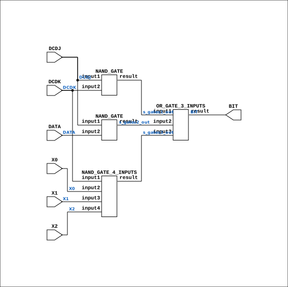
Contains: NAND_GATE x2, NAND_GATE_4_INPUTS, OR_GATE_3_INPUTS
Module hierarchy - All modules
Schematic
Drawn from the Verilog: the yosys netlist of the Simulation (Verilator) build, instance CORE.CPU_BOARD.CPU.PROC.CGA.DELILAH.INTR.CNTLR.CLR_CLEAR_CONTROL.CLRB3. Sub-modules are boxes (click the picture to open it full size; there every sub-module box links to its page, and every wire shows its Verilog name).
Description
ND120 CGA (CPU Gate Array / DELILAH) /CGA/INTR/CNTLR/CLR/CLRBIT CLRBIT Page 82 SHEET 1 of 1 Last reviewed: 10-NOV-2024 Ronny Hansen
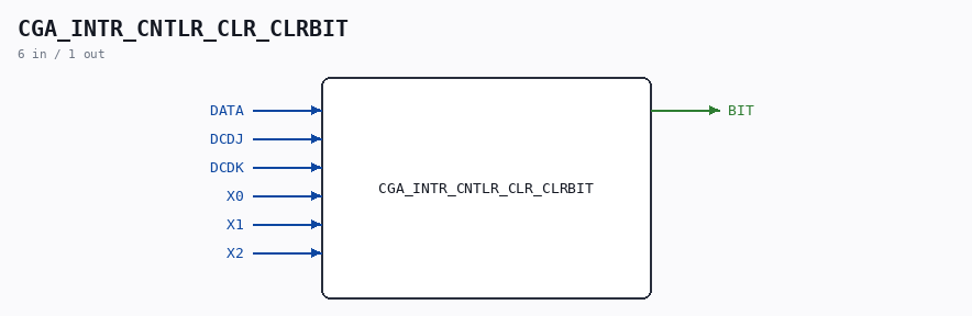
Ports
| Direction | Width | Name | Description |
|---|---|---|---|
| input | 1 |
DATA |
|
| input | 1 |
DCDJ |
|
| input | 1 |
DCDK |
|
| input | 1 |
X0 |
|
| input | 1 |
X1 |
|
| input | 1 |
X2 |
|
| output | 1 |
BIT |
Verilog source
Verilog/DELILAH-CPU/CGA_INTR/circuit/CGA_INTR_CNTLR_CLR_CLRBIT.v on GitHub.
Show the Verilog of CGA_INTR_CNTLR_CLR_CLRBIT (92 lines)
/**************************************************************************
** ND120 CGA (CPU Gate Array / DELILAH)                                  **
** /CGA/INTR/CNTLR/CLR/CLRBIT                                            **
** CLRBIT                                                                **
**                                                                       **
** Page 82                                                               **
** SHEET 1 of 1                                                          **
**                                                                       **
** Last reviewed: 10-NOV-2024                                            **
** Ronny Hansen                                                          **
***************************************************************************/

module CGA_INTR_CNTLR_CLR_CLRBIT (
    input DATA,
    input DCDJ,
    input DCDK,
    input X0,
    input X1,
    input X2,

    output BIT
);

  /*******************************************************************************
   ** The wires are defined here                                                 **
   *******************************************************************************/
  wire s_dcdj;
  wire s_dcdk;
  wire s_x2;
  wire s_gates3_out;
  wire s_bit_out;
  wire s_gates1_out;
  wire s_x0;
  wire s_x1;
  wire s_data;
  wire s_gates2_out;

  /*******************************************************************************
   ** Here all input connections are defined                                     **
   *******************************************************************************/
  assign s_dcdj = DCDJ;
  assign s_dcdk = DCDK;
  assign s_x2 = X2;
  assign s_x0 = X0;
  assign s_x1 = X1;
  assign s_data = DATA;

  /*******************************************************************************
   ** Here all output connections are defined                                    **
   *******************************************************************************/
  assign BIT = s_bit_out;

  /*******************************************************************************
   ** Here all normal components are defined                                     **
   *******************************************************************************/
  NAND_GATE #(
      .BubblesMask(2'b00)
  ) GATES_1 (
      .input1(s_dcdj),
      .input2(s_dcdk),
      .result(s_gates1_out)
  );

  NAND_GATE #(
      .BubblesMask(2'b00)
  ) GATES_2 (
      .input1(s_dcdj),
      .input2(s_data),
      .result(s_gates2_out)
  );

  NAND_GATE_4_INPUTS #(
      .BubblesMask(4'h0)
  ) GATES_3 (
      .input1(s_dcdk),
      .input2(s_x0),
      .input3(s_x1),
      .input4(s_x2),
      .result(s_gates3_out)
  );

  OR_GATE_3_INPUTS #(
      .BubblesMask(3'b111)
  ) GATES_4 (
      .input1(s_gates1_out),
      .input2(s_gates2_out),
      .input3(s_gates3_out),
      .result(s_bit_out)
  );


endmodule