CGA_INTR_CNTLR_IRQ_REG_RQBIT_V2
Source: Verilog/DELILAH-CPU/CGA_INTR/circuit/CGA_INTR_CNTLR_IRQ_REG_RQBIT_V2.v
Where it sits (Simulation): ND120_TOP > ND120_CORE > ND3202D > CPU_15 > CPU_PROC_32 > CPU_PROC_CGA_33 > CGA > CGA_INTR > CGA_INTR_CNTLR > CGA_INTR_CNTLR_IRQ > CGA_INTR_CNTLR_IRQ_REG > CGA_INTR_CNTLR_IRQ_REG_RQBIT_V2
- instance path: CORE.CPU_BOARD.CPU.PROC.CGA.DELILAH.INTR.CNTLR.IRQ.IRQ_REG.RQBIT_0
Used in: CGA_INTR_CNTLR_IRQ_REG (all tops)
Contains: D_FLIPFLOP_EN
Module hierarchy - All modules
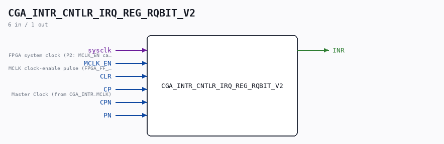
Schematic
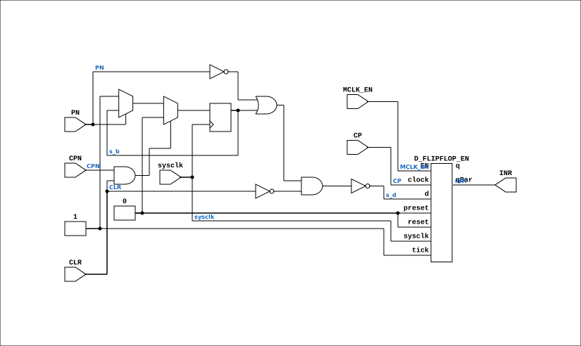
Drawn from the Verilog: the yosys netlist of the Simulation (Verilator) build, instance CORE.CPU_BOARD.CPU.PROC.CGA.DELILAH.INTR.CNTLR.IRQ.IRQ_REG.RQBIT_0. Sub-modules are boxes (click the picture to open it full size; there every sub-module box links to its page, and every wire shows its Verilog name).
Description
ND120 CGA (CPU Gate Array / DELILAH) /CGA/INTR/CNTLR/IRQ/REG/RQBIT_V2 INTERRUPT CONTROLLER REGISTER Q BIT - loop-free replacement Page 78 SHEET 1 of 1 Drop-in replacement for CGA_INTR_CNTLR_IRQ_REG_RQBIT with NO combinational feedback loop. The original holds the request in a cross-coupled OR/NAND SR latch (s_ff_or_out <-> s_ff_nand_out) that (a) yosys/nextpnr reject as a combinational loop, (b) oscillates from X-init in event simulators, and (c) is glitch-sensitive on real FPGA fabric. Contract (proved exhaustively against the gate netlist in ../sim/CGA_INTR_CNTLR_IRQ_REG_RQBIT_tb.v and the V2 equivalence tb): PN = interrupt request, ACTIVE-LOW (PN=0 -> request asserted) CLR = clear line, ACTIVE-HIGH (dominates) INR = latched request, ACTIVE-HIGH The async latch B catches a request pulse at ANY time (set on PN=0), is cleared by CLR while CP is low (CPN & CLR, clear dominates), and the output FF samples d = ~((~PN | B) & ~CLR) on each rising CP (= MCLK), INR = qBar. Implementation: B is replaced by a sysclk-clocked catcher flip-flop with the same set/clear priority - set when PN is low, cleared when CPN & CLR, clear dominating. It catches any request pulse of at least one sysclk cycle, which covers the real pulse sources (e.g. the one-cycle set-request pulses of a PID register write - measured in the system trace, levels pulse PN low for exactly one sysclk between MCLK edges). The output FF is the same D_FLIPFLOP_EN as the original, in the same two build modes (FPGA_FF_MODE: posedge sysclk gated by MCLK_EN; otherwise posedge CP). No combinational loop anywhere: both state elements are edge-triggered. Residual, intentional difference vs the async original (see ../sim/CGA_INTR_CNTLR_IRQ_REG_RQBIT_V2_tb.v): only events narrower than one sysclk cycle (combinational glitches / delta races) can be caught by the transparent latch and not by the catcher - on FPGA fabric that glitch sensitivity is exactly the failure mode this module removes. Last reviewed: 15-JUL-2026 Ronny Hansen
Ports
| Direction | Width | Name | Description |
|---|---|---|---|
| input | 1 |
sysclk |
FPGA system clock (P2: MCLK_EN capture) |
| input | 1 |
MCLK_EN |
MCLK clock-enable pulse (FPGA_FF_MODE, else 0) |
| input | 1 |
CLR |
|
| input | 1 |
CP |
Master Clock (from CGA_INTR.MCLK) |
| input | 1 |
CPN |
|
| input | 1 |
PN |
|
| output | 1 |
INR |
Verilog source
Verilog/DELILAH-CPU/CGA_INTR/circuit/CGA_INTR_CNTLR_IRQ_REG_RQBIT_V2.v on GitHub.
Show the Verilog of CGA_INTR_CNTLR_IRQ_REG_RQBIT_V2 (119 lines)
/**************************************************************************
** ND120 CGA (CPU Gate Array / DELILAH)                                  **
** /CGA/INTR/CNTLR/IRQ/REG/RQBIT_V2                                      **
** INTERRUPT CONTROLLER REGISTER Q BIT - loop-free replacement           **
**                                                                       **
** Page 78                                                               **
** SHEET 1 of 1                                                          **
**                                                                       **
** Drop-in replacement for CGA_INTR_CNTLR_IRQ_REG_RQBIT with NO          **
** combinational feedback loop. The original holds the request in a      **
** cross-coupled OR/NAND SR latch (s_ff_or_out <-> s_ff_nand_out) that   **
** (a) yosys/nextpnr reject as a combinational loop, (b) oscillates      **
** from X-init in event simulators, and (c) is glitch-sensitive on       **
** real FPGA fabric.                                                     **
**                                                                       **
** Contract (proved exhaustively against the gate netlist in             **
** ../sim/CGA_INTR_CNTLR_IRQ_REG_RQBIT_tb.v and the V2 equivalence tb):  **
**   PN  = interrupt request, ACTIVE-LOW  (PN=0 -> request asserted)     **
**   CLR = clear line,        ACTIVE-HIGH (dominates)                    **
**   INR = latched request,   ACTIVE-HIGH                                **
**   The async latch B catches a request pulse at ANY time (set on       **
**   PN=0), is cleared by CLR while CP is low (CPN & CLR, clear          **
**   dominates), and the output FF samples                               **
**   d = ~((~PN | B) & ~CLR) on each rising CP (= MCLK), INR = qBar.     **
**                                                                       **
** Implementation: B is replaced by a sysclk-clocked catcher flip-flop   **
** with the same set/clear priority - set when PN is low, cleared when   **
** CPN & CLR, clear dominating. It catches any request pulse of at       **
** least one sysclk cycle, which covers the real pulse sources (e.g.     **
** the one-cycle set-request pulses of a PID register write - measured   **
** in the system trace, levels pulse PN low for exactly one sysclk       **
** between MCLK edges). The output FF is the same D_FLIPFLOP_EN as the   **
** original, in the same two build modes (FPGA_FF_MODE: posedge sysclk   **
** gated by MCLK_EN; otherwise posedge CP). No combinational loop        **
** anywhere: both state elements are edge-triggered.                     **
**                                                                       **
** Residual, intentional difference vs the async original (see           **
** ../sim/CGA_INTR_CNTLR_IRQ_REG_RQBIT_V2_tb.v): only events narrower    **
** than one sysclk cycle (combinational glitches / delta races) can be   **
** caught by the transparent latch and not by the catcher - on FPGA      **
** fabric that glitch sensitivity is exactly the failure mode this      **
** module removes.                                                       **
**                                                                       **
** Last reviewed: 15-JUL-2026                                            **
** Ronny Hansen                                                          **
***************************************************************************/

module CGA_INTR_CNTLR_IRQ_REG_RQBIT_V2 (
    input sysclk,   //! FPGA system clock (P2: MCLK_EN capture)
    input MCLK_EN,  //! MCLK clock-enable pulse (FPGA_FF_MODE, else 0)

    input CLR,
    input CP,       //! Master Clock (from CGA_INTR.MCLK)
    input CPN,
    input PN,

    output INR
);

  /*******************************************************************************
   ** The wires are defined here                                                 **
   *******************************************************************************/
  wire s_d;
  wire s_inr_out;

  /*******************************************************************************
   ** The module functionality is described here                                 **
   *******************************************************************************/

  // P2 (docs/plan-fix-unconstrained-clocks.md): in FF mode the MCLK-
  // clocked registers capture on posedge sysclk gated by MCLK_EN
  // (aligned to the MCLK rise) instead of clocking on the routed net.
`ifdef FPGA_FF_MODE
  localparam MCLK_CE = 1;
`else
  localparam MCLK_CE = 0;
`endif

  /*******************************************************************************
   ** Here all output connections are defined                                    **
   *******************************************************************************/
  assign INR = s_inr_out;

  /*******************************************************************************
   ** Here all normal components are defined                                     **
   *******************************************************************************/

  // Request pulse catcher: replicates the async SR latch at sysclk
  // granularity with no combinational loop. Set by an active request
  // (PN low) at any time; cleared when CLR is asserted while the MCLK
  // phase is low (CPN & CLR) - clear dominates, matching the gate
  // priority of the original latch. Catches any request pulse of at
  // least one sysclk cycle (e.g. PID-write set pulses).
  reg s_b = 1'b0;
  always @(posedge sysclk) begin
    if (CPN & CLR) s_b <= 1'b0;
    else if (!PN)  s_b <= 1'b1;
  end

  // Same D function as the original's GATES_3: clear dominates; a live
  // or caught request sets; otherwise the caught state holds.
  assign s_d = ~((~PN | s_b) & ~CLR);

  // CP resolves to MCLK (CGA_INTR.MCLK, rising edge) - MCLK domain
  D_FLIPFLOP_EN #(
      .USE_ENABLE(MCLK_CE)
  ) MEMORY_1 (
      .sysclk(sysclk),
      .EN(MCLK_EN),
      .clock(CP),
      .d(s_d),
      .preset(1'b0),
      .q(),
      .qBar(s_inr_out),
      .reset(1'b0),
      .tick(1'b1)
  );

endmodule