CGA_MIC_MASEL
Source: Verilog/DELILAH-CPU/CGA_MIC/circuit/CGA_MIC_MASEL.v
Where it sits (Simulation): ND120_TOP > ND120_CORE > ND3202D > CPU_15 > CPU_PROC_32 > CPU_PROC_CGA_33 > CGA > CGA_MIC > CGA_MIC_MASEL
- instance path: CORE.CPU_BOARD.CPU.PROC.CGA.DELILAH.MIC.MIC_MASEL
Used in: CGA_MIC (all tops)
Contains: no other modules.
Module hierarchy - All modules
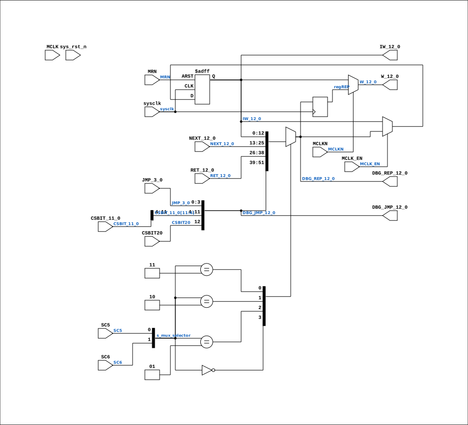
Schematic
Drawn from the Verilog: the yosys netlist of the Simulation (Verilator) build, instance CORE.CPU_BOARD.CPU.PROC.CGA.DELILAH.MIC.MIC_MASEL. Sub-modules are boxes (click the picture to open it full size; there every sub-module box links to its page, and every wire shows its Verilog name).
Description
ND120 CGA (CPU Gate Array / DELILAH) /CGA/MIC/MASEL Microcode Address SELECT Page 19 SHEET 1 of 1 Last reviewed: 22-MARCH 2025 Ronny Hansen
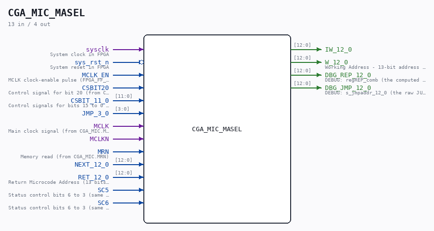
Ports
| Direction | Width | Name | Description |
|---|---|---|---|
| input | 1 |
sysclk |
System clock in FPGA |
| input | 1 |
sys_rst_n (active low) |
System reset in FPGA |
| input | 1 |
MCLK_EN |
MCLK clock-enable pulse (FPGA_FF_MODE, else 0) |
| input | 1 |
CSBIT20 |
Control signal for bit 20 (from CGA_MIC.CSBIT20) |
| input | [11:0] |
CSBIT_11_0 |
Control signals for bits 15 to 0 (from CGA_MIC.CSBIT_15_0[11:0]) |
| input | [3:0] |
JMP_3_0 |
|
| input | 1 |
MCLK |
Main clock signal (from CGA_MIC.MCLK) |
| input | 1 |
MCLKN |
|
| input | 1 |
MRN |
Memory read (from CGA_MIC.MRN) |
| input | [12:0] |
NEXT_12_0 |
|
| input | [12:0] |
RET_12_0 |
Return Microcode Address (13 bits) (from CGA_MIC_STACK.RET_12_0) |
| input | 1 |
SC5 |
Status control bits 6 to 3 (same net as CGA_MIC.SC_6_3[2]) |
| input | 1 |
SC6 |
Status control bits 6 to 3 (same net as CGA_MIC.SC_6_3[3]) |
| output | [12:0] |
IW_12_0 |
|
| output | [12:0] |
W_12_0 |
Working Address - 13-bit address used during normal operation (to CGA_MIC_IPOS.W_12_0) |
| output | [12:0] |
DBG_REP_12_0 |
DEBUG: regREP_comb (the computed next-address the sequencer selected; for SEL_JUMP = s_jmpaddr). Tang 06000-hang root-cause. |
| output | [12:0] |
DBG_JMP_12_0 |
DEBUG: s_jmpaddr_12_0 (the raw JUMP target = {csbit20,csbit_11_0[11:4],jmp}). If wrong => WCS-read/CSBITS wrong. |
Verilog source
Verilog/DELILAH-CPU/CGA_MIC/circuit/CGA_MIC_MASEL.v on GitHub.
Show the Verilog of CGA_MIC_MASEL (414 lines)
/**************************************************************************
** ND120 CGA (CPU Gate Array / DELILAH)                                  **
** /CGA/MIC/MASEL                                                        **
** Microcode Address SELECT                                              **
**                                                                       **
** Page 19                                                               **
** SHEET 1 of 1                                                          **
**                                                                       **
** Last reviewed: 22-MARCH 2025                                             **
** Ronny Hansen                                                          **
***************************************************************************/

module CGA_MIC_MASEL (
    input sysclk,    // System clock in FPGA
    input sys_rst_n, // System reset in FPGA

    input        MCLK_EN,  //! MCLK clock-enable pulse (FPGA_FF_MODE, else 0)

    input        CSBIT20,  //! Control signal for bit 20 (from CGA_MIC.CSBIT20)
    input [11:0] CSBIT_11_0,  //! Control signals for bits 15 to 0 (from CGA_MIC.CSBIT_15_0[11:0])
    input [ 3:0] JMP_3_0,
    input        MCLK,  //! Main clock signal (from CGA_MIC.MCLK)
    input        MCLKN,
    input        MRN,  //! Memory read (from CGA_MIC.MRN)
    input [12:0] NEXT_12_0,
    input [12:0] RET_12_0,  //! Return Microcode Address (13 bits) (from CGA_MIC_STACK.RET_12_0)
    input        SC5,  //! Status control bits 6 to 3 (same net as CGA_MIC.SC_6_3[2])
    input        SC6,  //! Status control bits 6 to 3 (same net as CGA_MIC.SC_6_3[3])

    output [12:0] IW_12_0,
    output [12:0] W_12_0,  //! Working Address - 13-bit address used during normal operation (to CGA_MIC_IPOS.W_12_0)
    output [12:0] DBG_REP_12_0,  //! DEBUG: regREP_comb (the computed next-address the sequencer selected; for SEL_JUMP = s_jmpaddr). Tang 06000-hang root-cause.
    output [12:0] DBG_JMP_12_0   //! DEBUG: s_jmpaddr_12_0 (the raw JUMP target = {csbit20,csbit_11_0[11:4],jmp}). If wrong => WCS-read/CSBITS wrong.
);

localparam [1:0] SEL_JUMP   = 2'b00;
localparam [1:0] SEL_RETURN = 2'b01;
localparam [1:0] SEL_NEXT   = 2'b10;
localparam [1:0] SEL_REPEAT = 2'b11;


  /*******************************************************************************
   ** The wires are defined here                                                 **
   *******************************************************************************/
  (* mark_debug = "true", DONT_TOUCH = "true" *) wire [ 1:0] s_mux_selector;
  wire [12:0] s_ret_12_0;
  wire [12:0] s_next_12_0;
  (* mark_debug = "true", DONT_TOUCH = "true" *) wire [11:0] s_csbit_11_0;
  wire [12:0] s_w_12_0_out;
  wire [12:0] s_iw_12_0_out;
  (* mark_debug = "true", DONT_TOUCH = "true" *) wire [ 3:0] s_jmp_3_0;
  //wire [12:0] s_rep_12_0;
  (* mark_debug = "true", DONT_TOUCH = "true" *) wire        s_csbit20;
  wire        s_mclk_n;
  wire        s_mclk;
  wire        s_mr_n;

  /*******************************************************************************
   ** The module functionality is described here                                 **
   *******************************************************************************/

  /*******************************************************************************
   ** Here all input connections are defined                                     **
   *******************************************************************************/
  assign s_mux_selector[0]  = SC5;
  assign s_mux_selector[1]  = SC6;
  assign s_ret_12_0[12:0]   = RET_12_0;
  assign s_next_12_0[12:0]  = NEXT_12_0;
  assign s_csbit_11_0[11:0] = CSBIT_11_0;
  assign s_jmp_3_0[3:0]     = JMP_3_0;
  assign s_mclk_n           = MCLKN;
  assign s_mclk             = MCLK;
  assign s_csbit20          = CSBIT20;
  assign s_mr_n             = MRN;

  (* mark_debug = "true", DONT_TOUCH = "true" *) wire [12:0] s_jmpaddr_12_0;
  // Fixed: Added s_csbit20 as bit 12 for complete 13-bit assignment
  assign s_jmpaddr_12_0 = {s_csbit20, s_csbit_11_0[11:4], s_jmp_3_0[3:0]};

  /*******************************************************************************
   ** Here all output connections are defined                                    **
   *******************************************************************************/
  // assign IW_12_0            = s_iw_12_0_out[12:0];
  //assign W_12_0             = s_w_12_0_out[12:0];

  // Register declarations (moved before assign to avoid synthesis warning)
  (* mark_debug = "true", DONT_TOUCH = "true" *) reg [12:0] regREP;
  (* mark_debug = "true", DONT_TOUCH = "true" *) reg [12:0] regW;
  (* mark_debug = "true", DONT_TOUCH = "true" *) reg [12:0] regIW;

  assign IW_12_0            = regIW;
  assign W_12_0             = regW;
  assign DBG_REP_12_0       = regREP_comb;  // computed next-address (JUMP target when SC=JUMP)
  assign DBG_JMP_12_0       = s_jmpaddr_12_0; // raw JUMP target (from csbits) - wrong => WCS/CSBITS bad

  // Code to make LINTER _not_ complain about bits not read in CSBIITS bits 3:0
  (* keep = "true", DONT_TOUCH = "true" *) wire [3:0] unused_CSBITS_bits;
  assign unused_CSBITS_bits[3:0] = s_csbit_11_0[3:0];

  // VARIANT F: register regREP through sysclk to break the data race.
  // The combinational mux output feeds a 1-sysclk pipeline register.
  // regIW then captures from the registered (stable) regREP at
  // posedge s_mclk without a setup violation.
  reg [12:0] regREP_comb;
  always @(*) begin
    case (s_mux_selector)
        SEL_JUMP: begin
            // handle jump
            regREP_comb = s_jmpaddr_12_0;
        end
        SEL_RETURN: begin
            // handle return
            regREP_comb = s_ret_12_0;
        end
        SEL_NEXT: begin
            // handle next
            regREP_comb = s_next_12_0;
        end
        SEL_REPEAT: begin
            // handle repeat
            regREP_comb = IW_12_0;
        end
        default: begin
            // optional: handle invalid case
            regREP_comb = s_next_12_0;
        end
    endcase
  end

  always @(posedge sysclk) begin
    regREP <= regREP_comb;
  end

  // LATCH regREP to W as long as MCLKN is active
  // Is used by IPOS to create the MA_12_0 address to microcode RAM
  // Fixed: Converted latch to combinational logic - when s_mclk_n is low, use registered value
  always @(*) begin
    if (s_mclk_n) begin
      regW = regREP;  // Transparent when clock is high
    end else begin
      regW = regIW;   // Use registered value when clock is low (holds last captured value)
    end
  end


  // On rising clock edge load REP into IW
  // IW goes back to IINC to calculate next address (which is then input to stack module)
  // MCLK domain: regIW clocks on posedge s_mclk (async clear s_mr_n).
  // P2 (docs/plan-fix-unconstrained-clocks.md): in FF mode capture on
  // posedge sysclk gated by MCLK_EN (aligned to the MCLK rise) instead
  // of clocking on the routed net.
`ifdef FPGA_FF_MODE
  /* verilator lint_off UNUSEDSIGNAL */
  wire unused_mclk = s_mclk;
  /* verilator lint_on UNUSEDSIGNAL */
  // regREP is itself a sysclk register updating on EVERY posedge (VARIANT F
  // above): the original pa-clocked regIW fired a delta AFTER that update
  // and so captured regREP's NEW value. Sampling regREP here (pre-edge NBA)
  // would be one cycle stale - capture the register's D input regREP_comb
  // instead, which is exactly the value the original saw.
  always @(posedge sysclk or negedge s_mr_n) begin
    if (!s_mr_n) begin
        regIW <= 0;
    end else if (MCLK_EN) begin
      regIW <= regREP_comb;
    end
  end
`else
  /* verilator lint_off UNUSEDSIGNAL */
  wire unused_mclk_en = MCLK_EN;
  /* verilator lint_on UNUSEDSIGNAL */
  always @(posedge s_mclk or negedge s_mr_n) begin
    if (!s_mr_n) begin
        regIW <= 0;
    end else begin
      regIW <= regREP;
    end
  end
`endif


  /*******************************************************************************
   ** Here all normal components are defined                                     **
   *******************************************************************************/
   /*

   reg [12:0] dRep12;

  Multiplexer_4 PLEXERS_1 (
      .muxIn_0(s_csbit_11_0[11]),
      .muxIn_1(s_ret_12_0[11]),
      .muxIn_2(s_next_12_0[11]),
      .muxIn_3(s_iw_12_0_out[11]),
      .muxOut(s_rep_12_0[11]),
      .sel(s_mux_selector[1:0])
  );

  Multiplexer_4 PLEXERS_2 (
      .muxIn_0(s_csbit_11_0[10]),
      .muxIn_1(s_ret_12_0[10]),
      .muxIn_2(s_next_12_0[10]),
      .muxIn_3(s_iw_12_0_out[10]),
      .muxOut(s_rep_12_0[10]),
      .sel(s_mux_selector[1:0])
  );

  Multiplexer_4 PLEXERS_3 (
      .muxIn_0(s_csbit_11_0[9]),
      .muxIn_1(s_ret_12_0[9]),
      .muxIn_2(s_next_12_0[9]),
      .muxIn_3(s_iw_12_0_out[9]),
      .muxOut(s_rep_12_0[9]),
      .sel(s_mux_selector[1:0])
  );

  Multiplexer_4 PLEXERS_4 (
      .muxIn_0(s_csbit_11_0[8]),
      .muxIn_1(s_ret_12_0[8]),
      .muxIn_2(s_next_12_0[8]),
      .muxIn_3(s_iw_12_0_out[8]),
      .muxOut(s_rep_12_0[8]),
      .sel(s_mux_selector[1:0])
  );

  Multiplexer_4 PLEXERS_5 (
      .muxIn_0(s_csbit_11_0[7]),
      .muxIn_1(s_ret_12_0[7]),
      .muxIn_2(s_next_12_0[7]),
      .muxIn_3(s_iw_12_0_out[7]),
      .muxOut(s_rep_12_0[7]),
      .sel(s_mux_selector[1:0])
  );

  Multiplexer_4 PLEXERS_6 (
      .muxIn_0(s_csbit_11_0[6]),
      .muxIn_1(s_ret_12_0[6]),
      .muxIn_2(s_next_12_0[6]),
      .muxIn_3(s_iw_12_0_out[6]),
      .muxOut(s_rep_12_0[6]),
      .sel(s_mux_selector[1:0])
  );

  Multiplexer_4 PLEXERS_7 (
      .muxIn_0(s_csbit_11_0[5]),
      .muxIn_1(s_ret_12_0[5]),
      .muxIn_2(s_next_12_0[5]),
      .muxIn_3(s_iw_12_0_out[5]),
      .muxOut(s_rep_12_0[5]),
      .sel(s_mux_selector[1:0])
  );

  Multiplexer_4 PLEXERS_8 (
      .muxIn_0(s_csbit_11_0[4]),
      .muxIn_1(s_ret_12_0[4]),
      .muxIn_2(s_next_12_0[4]),
      .muxIn_3(s_iw_12_0_out[4]),
      .muxOut(s_rep_12_0[4]),
      .sel(s_mux_selector[1:0])
  );

  Multiplexer_4 PLEXERS_9 (
      .muxIn_0(s_jmp_3_0[3]),
      .muxIn_1(s_ret_12_0[3]),
      .muxIn_2(s_next_12_0[3]),
      .muxIn_3(s_iw_12_0_out[3]),
      .muxOut(s_rep_12_0[3]),
      .sel(s_mux_selector[1:0])
  );

  Multiplexer_4 PLEXERS_10 (
      .muxIn_0(s_jmp_3_0[2]),
      .muxIn_1(s_ret_12_0[2]),
      .muxIn_2(s_next_12_0[2]),
      .muxIn_3(s_iw_12_0_out[2]),
      .muxOut(s_rep_12_0[2]),
      .sel(s_mux_selector[1:0])
  );

  Multiplexer_4 PLEXERS_11 (
      .muxIn_0(s_jmp_3_0[1]),
      .muxIn_1(s_ret_12_0[1]),
      .muxIn_2(s_next_12_0[1]),
      .muxIn_3(s_iw_12_0_out[1]),
      .muxOut(s_rep_12_0[1]),
      .sel(s_mux_selector[1:0])
  );

  Multiplexer_4 PLEXERS_12 (
      .muxIn_0(s_jmp_3_0[0]),
      .muxIn_1(s_ret_12_0[0]),
      .muxIn_2(s_next_12_0[0]),
      .muxIn_3(s_iw_12_0_out[0]),
      .muxOut(s_rep_12_0[0]),
      .sel(s_mux_selector[1:0])
  );

  Multiplexer_4 PLEXERS_13 (
      .muxIn_0(s_csbit20),
      .muxIn_1(s_ret_12_0[12]),
      .muxIn_2(s_next_12_0[12]),
      .muxIn_3(s_iw_12_0_out[12]),
      .muxOut(s_rep_12_0[12]),
      .sel(s_mux_selector[1:0])
  );

*/

  /*******************************************************************************
   ** Here all sub-circuits are defined                                          **
   *******************************************************************************/
/*
  L8 WL_HI
  (
    // System Input signals
    .sysclk(sysclk),                          // System clock in FPGA
    .sys_rst_n(sys_rst_n),                    // System reset in FPGA

    // Input signals
    .L  (s_mclk_n),

    .A  (s_rep_12_0[12]),
    .B  (s_rep_12_0[11]),
    .C  (s_rep_12_0[10]),
    .D  (s_rep_12_0[9]),
    .E  (s_rep_12_0[8]),
    .F  (s_rep_12_0[7]),
    .G  (s_rep_12_0[6]),
    .H  (s_rep_12_0[5]),

    // Output signals
    .QA (s_w_12_0_out[12]),
    .QAN(),
    .QB (s_w_12_0_out[11]),
    .QBN(),
    .QC (s_w_12_0_out[10]),
    .QCN(),
    .QD (s_w_12_0_out[9]),
    .QDN(),
    .QE (s_w_12_0_out[8]),
    .QEN(),
    .QF (s_w_12_0_out[7]),
    .QFN(),
    .QG (s_w_12_0_out[6]),
    .QGN(),
    .QH (s_w_12_0_out[5]),
    .QHN()
  );

  L8 WL_LO
  (
    // System Input signals
    .sysclk(sysclk),                          // System clock in FPGA
    .sys_rst_n(sys_rst_n),                    // System reset in FPGA

    // Input signals
    .L  (s_mclk_n),

    .A  (s_rep_12_0[4]),
    .B  (s_rep_12_0[3]),
    .C  (s_rep_12_0[2]),
    .D  (s_rep_12_0[1]),
    .E  (s_rep_12_0[0]),
    .F  (1'b0),
    .G  (1'b0),
    .H  (1'b0),

    // Output signals
    .QA (s_w_12_0_out[4]),
    .QAN(),
    .QB (s_w_12_0_out[3]),
    .QBN(),
    .QC (s_w_12_0_out[2]),
    .QCN(),
    .QD (s_w_12_0_out[1]),
    .QDN(),
    .QE (s_w_12_0_out[0]),
    .QEN(),
    .QF (),
    .QFN(),
    .QG (),
    .QGN(),
    .QH (),
    .QHN()
  );

  //always @(negedge sysclk) begin
  always @(posedge sysclk) begin
    if (!sys_rst_n) begin
        dRep12[12:0] <=0;
    end else begin
        dRep12[12:0] <= s_rep_12_0[12:0];
    end
  end

  wire rptClock;
  assign rptClock = s_mclk;


  CGA_MIC_MASEL_REPEAT MASEL_REPEAT (
      .SC6(SC6),
      .SC5(SC5),
      .IW_12_0(s_iw_12_0_out[12:0]),
      //.MCLK(s_mclk),
      .MCLK(rptClock),
      .MPN(s_mr_n),
      .REP_12_0(s_w_12_0_out)
      //.REP_12_0(s_rep_12_0[12:0])
      //.REP_12_0(dRep12[12:0])
  );
  */

endmodule