CGA
Source: Verilog/DELILAH-CPU/CGA/circuit/CGA.v
Where it sits (Simulation): ND120_TOP > ND120_CORE > ND3202D > CPU_15 > CPU_PROC_32 > CPU_PROC_CGA_33 > CGA
- instance path: CORE.CPU_BOARD.CPU.PROC.CGA.DELILAH
Used in: CPU_PROC_CGA_33 (all tops)
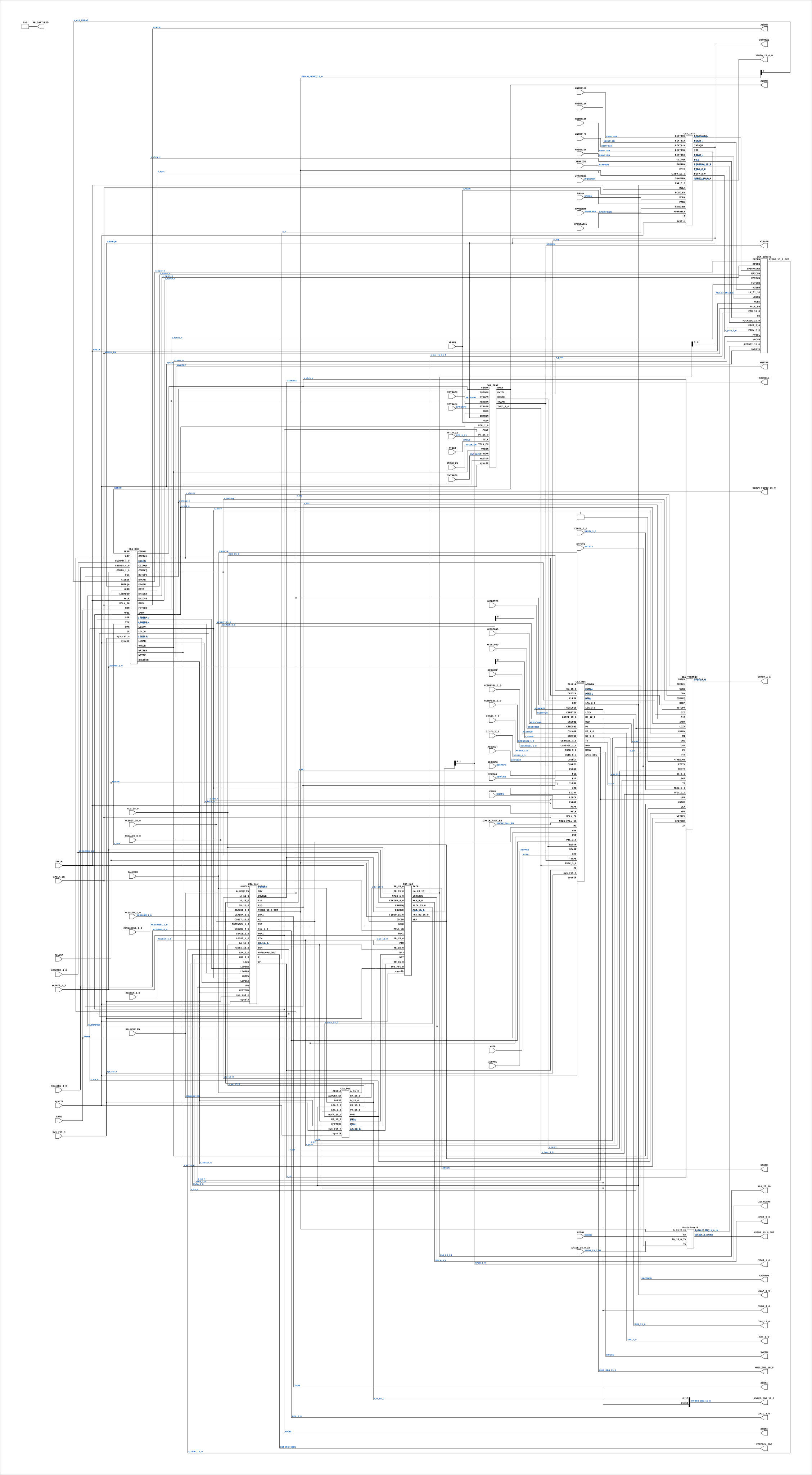
Contains: BusDriver16, CGA_ALU, CGA_DCD, CGA_IDBCTL, CGA_INTR, CGA_MAC, CGA_MIC, CGA_TESTMUX, CGA_TRAP, CGA_WRF
Module hierarchy - All modules
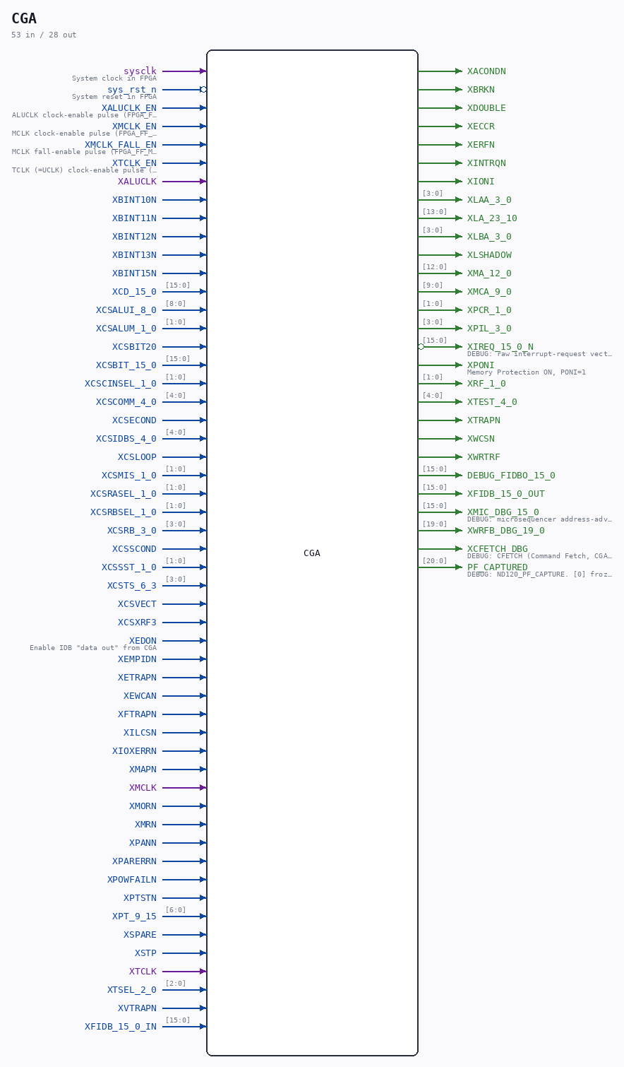
Schematic
Drawn from the Verilog: the yosys netlist of the Simulation (Verilator) build, instance CORE.CPU_BOARD.CPU.PROC.CGA.DELILAH. Sub-modules are boxes (click the picture to open it full size; there every sub-module box links to its page, and every wire shows its Verilog name).
Description
ND120 CGA (CPU Gate Array / DELILAH) /CGA CGA TOP LEVEL Page 2-9 SHEET 1 of 8 Last reviewed: 9-FEB-2025 Ronny Hansen
Ports
| Direction | Width | Name | Description |
|---|---|---|---|
| input | 1 |
sysclk |
System clock in FPGA |
| input | 1 |
sys_rst_n (active low) |
System reset in FPGA |
| input | 1 |
XALUCLK_EN |
ALUCLK clock-enable pulse (FPGA_FF_MODE, else 0) |
| input | 1 |
XMCLK_EN |
MCLK clock-enable pulse (FPGA_FF_MODE, else 0) |
| input | 1 |
XMCLK_FALL_EN |
MCLK fall-enable pulse (FPGA_FF_MODE, else 0) |
| input | 1 |
XTCLK_EN |
TCLK (=UCLK) clock-enable pulse (FPGA_FF_MODE, else 0) |
| input | 1 |
XALUCLK |
|
| input | 1 |
XBINT10N |
|
| input | 1 |
XBINT11N |
|
| input | 1 |
XBINT12N |
|
| input | 1 |
XBINT13N |
|
| input | 1 |
XBINT15N |
|
| input | [15:0] |
XCD_15_0 |
|
| input | [8:0] |
XCSALUI_8_0 |
|
| input | [1:0] |
XCSALUM_1_0 |
|
| input | 1 |
XCSBIT20 |
|
| input | [15:0] |
XCSBIT_15_0 |
|
| input | [1:0] |
XCSCINSEL_1_0 |
|
| input | [4:0] |
XCSCOMM_4_0 |
|
| input | 1 |
XCSECOND |
|
| input | [4:0] |
XCSIDBS_4_0 |
|
| input | 1 |
XCSLOOP |
|
| input | [1:0] |
XCSMIS_1_0 |
|
| input | [1:0] |
XCSRASEL_1_0 |
|
| input | [1:0] |
XCSRBSEL_1_0 |
|
| input | [3:0] |
XCSRB_3_0 |
|
| input | 1 |
XCSSCOND |
|
| input | [1:0] |
XCSSST_1_0 |
|
| input | [3:0] |
XCSTS_6_3 |
|
| input | 1 |
XCSVECT |
|
| input | 1 |
XCSXRF3 |
|
| input | 1 |
XEDON |
Enable IDB "data out" from CGA |
| input | 1 |
XEMPIDN |
|
| input | 1 |
XETRAPN |
|
| input | 1 |
XEWCAN |
|
| input | 1 |
XFTRAPN |
|
| input | 1 |
XILCSN |
|
| input | 1 |
XIOXERRN |
|
| input | 1 |
XMAPN |
|
| input | 1 |
XMCLK |
|
| input | 1 |
XMORN |
|
| input | 1 |
XMRN |
|
| input | 1 |
XPANN |
|
| input | 1 |
XPARERRN |
|
| input | 1 |
XPOWFAILN |
|
| input | 1 |
XPTSTN |
|
| input | [6:0] |
XPT_9_15 |
|
| input | 1 |
XSPARE |
|
| input | 1 |
XSTP |
|
| input | 1 |
XTCLK |
|
| input | [2:0] |
XTSEL_2_0 |
|
| input | 1 |
XVTRAPN |
|
| input | [15:0] |
XFIDB_15_0_IN |
|
| output | 1 |
XACONDN |
|
| output | 1 |
XBRKN |
|
| output | 1 |
XDOUBLE |
|
| output | 1 |
XECCR |
|
| output | 1 |
XERFN |
|
| output | 1 |
XINTRQN |
|
| output | 1 |
XIONI |
|
| output | [3:0] |
XLAA_3_0 |
|
| output | [13:0] |
XLA_23_10 |
|
| output | [3:0] |
XLBA_3_0 |
|
| output | 1 |
XLSHADOW |
|
| output | [12:0] |
XMA_12_0 |
|
| output | [9:0] |
XMCA_9_0 |
|
| output | [1:0] |
XPCR_1_0 |
|
| output | [3:0] |
XPIL_3_0 |
|
| output | [15:0] |
XIREQ_15_0_N (active low) |
DEBUG: raw interrupt-request vector (active low) |
| output | 1 |
XPONI |
Memory Protection ON, PONI=1 |
| output | [1:0] |
XRF_1_0 |
|
| output | [4:0] |
XTEST_4_0 |
|
| output | 1 |
XTRAPN |
|
| output | 1 |
XWCSN |
|
| output | 1 |
XWRTRF |
|
| output | [15:0] |
DEBUG_FIDBO_15_0 |
|
| output | [15:0] |
XFIDB_15_0_OUT |
|
| output | [15:0] |
XMIC_DBG_15_0 |
DEBUG: microsequencer address-advance probe (Tang 06000-hang) |
| output | [19:0] |
XWRFB_DBG_19_0 |
|
| output | 1 |
XCFETCH_DBG |
DEBUG: CFETCH (Command Fetch, CGA_DCD registered) - one rise |
| output | [20:0] |
PF_CAPTURED |
DEBUG: ND120_PF_CAPTURE. [0] froze (1 once the targeted fault/access happened |
Verilog source
Verilog/DELILAH-CPU/CGA/circuit/CGA.v on GitHub.
Show the Verilog of CGA (1836 lines)
/**************************************************************************
** ND120 CGA (CPU Gate Array / DELILAH) **
** /CGA **
** CGA TOP LEVEL **
** **
** Page 2-9 **
** SHEET 1 of 8 **
** **
** Last reviewed: 9-FEB-2025 **
** Ronny Hansen **
***************************************************************************/
// Both the PC-history ring and the JPL-read capture export the (fetch-
// qualified) P register on the CGA's single 16-bit debug port. The define has
// to be established BEFORE the first `ifdef that tests it - the MIC port
// intercept near the top of the module - so it lives here, not next to the
// probe itself.
`ifdef TANG_PC_HISTORY
`define ND120_PC_ON_DBG_PORT
`endif
`ifdef TANG_JPL_CAPTURE
`define ND120_PC_ON_DBG_PORT
`endif
// TANG_PTWR_CAPTURE's ERRFATAL trigger compares XMIC_DBG against the printer
// loop's P (004546), so it needs the P register on the port too. Run 1 of
// that variant (23-AUG) never dumped BECAUSE this define was missing: the
// port carried the microsequencer probe and the compare could never match.
`ifdef TANG_PTWR_CAPTURE
`define ND120_PC_ON_DBG_PORT
`endif
// TANG_PFPATH_CAPTURE (23-AUG): P register on the port AND the freeze register
// instantiated (readout NOT on the port) so its `captured` flag can trigger
// the top-level ring on the first no-permit access to the 0o1032 page.
`ifdef TANG_PFPATH_CAPTURE
`define ND120_PC_ON_DBG_PORT
`define ND120_PF_CAPTURE_INST
`endif
// TANG_PTORD_CAPTURE (23-AUG, Phase 1b): needs BOTH - the P register on the
// port for the ERRFATAL trigger, and the freeze register instantiated so its
// evt_noperm / evt_fault pulses can be interleaved with the page-table write
// stream in the top-level ring.
`ifdef TANG_PTORD_CAPTURE
`define ND120_PC_ON_DBG_PORT
`define ND120_PF_CAPTURE_INST
`endif
// TANG_PFLOG_CAPTURE (23-AUG, run 11): same pair of needs - P on the port for
// the ERRFATAL trigger, freeze register instantiated for the fault stream.
`ifdef TANG_PFLOG_CAPTURE
`define ND120_PC_ON_DBG_PORT
`define ND120_PF_CAPTURE_INST
`endif
// TANG_PGW_CAPTURE (24-AUG, run 16): the ERRFATAL trigger compares XMIC_DBG
// against the printer loop's P, so the P register must be on the debug port.
`ifdef TANG_PGW_CAPTURE
`define ND120_PC_ON_DBG_PORT
`endif
`ifdef TANG_PF_CAPTURE
`define ND120_PF_CAPTURE_INST
`endif
module CGA (
// System input signals
input sysclk, // System clock in FPGA
input sys_rst_n, // System reset in FPGA
// Control and data inputs
input XALUCLK_EN, //! ALUCLK clock-enable pulse (FPGA_FF_MODE, else 0)
input XMCLK_EN, //! MCLK clock-enable pulse (FPGA_FF_MODE, else 0)
input XMCLK_FALL_EN, //! MCLK fall-enable pulse (FPGA_FF_MODE, else 0)
input XTCLK_EN, //! TCLK (=UCLK) clock-enable pulse (FPGA_FF_MODE, else 0)
input XALUCLK,
input XBINT10N,
input XBINT11N,
input XBINT12N,
input XBINT13N,
input XBINT15N,
input [15:0] XCD_15_0,
input [ 8:0] XCSALUI_8_0,
input [ 1:0] XCSALUM_1_0,
input XCSBIT20,
input [15:0] XCSBIT_15_0,
input [ 1:0] XCSCINSEL_1_0,
input [ 4:0] XCSCOMM_4_0,
input XCSECOND,
input [ 4:0] XCSIDBS_4_0,
input XCSLOOP,
input [ 1:0] XCSMIS_1_0,
input [ 1:0] XCSRASEL_1_0,
input [ 1:0] XCSRBSEL_1_0,
input [ 3:0] XCSRB_3_0,
input XCSSCOND,
input [ 1:0] XCSSST_1_0,
input [ 3:0] XCSTS_6_3,
input XCSVECT,
input XCSXRF3,
input XEDON, //! Enable IDB "data out" from CGA
input XEMPIDN,
input XETRAPN,
input XEWCAN,
input XFTRAPN,
input XILCSN,
input XIOXERRN,
input XMAPN,
input XMCLK,
input XMORN,
input XMRN,
input XPANN,
input XPARERRN,
input XPOWFAILN,
input XPTSTN,
input [ 6:0] XPT_9_15,
input XSPARE,
input XSTP,
input XTCLK,
input [ 2:0] XTSEL_2_0,
input XVTRAPN,
input [15:0] XFIDB_15_0_IN,
// Control and data outputs
output XACONDN,
output XBRKN,
output XDOUBLE,
output XECCR,
output XERFN,
output XINTRQN,
output XIONI,
output [ 3:0] XLAA_3_0,
output [13:0] XLA_23_10,
output [ 3:0] XLBA_3_0,
output XLSHADOW,
output [12:0] XMA_12_0,
output [ 9:0] XMCA_9_0,
output [ 1:0] XPCR_1_0,
output [ 3:0] XPIL_3_0,
output [15:0] XIREQ_15_0_N, //! DEBUG: raw interrupt-request vector (active low)
output XPONI, //! Memory Protection ON, PONI=1
output [ 1:0] XRF_1_0,
output [ 4:0] XTEST_4_0,
output XTRAPN,
output XWCSN,
output XWRTRF,
// Debug
output [15:0] DEBUG_FIDBO_15_0,
output [15:0] XFIDB_15_0_OUT,
output [15:0] XMIC_DBG_15_0, //! DEBUG: microsequencer address-advance probe (Tang 06000-hang)
//! DEBUG: the register-file B PORT, as {LBA_3_0, B_15_0}. Added 01-SEP-2026
//! for the MiSTer bring-up: the self-test failure path is
//! STERR: B,R2 ALUF,PASSB ALUD,Q ... (microcode 002156)
//! which puts the error number - held in R2 - onto this very port. Latching
//! it at CSA==002156 therefore reads the error number WITHOUT needing to
//! know which of the 16 register slots the assembler's "R2" decodes to, and
//! the LBA half reports that slot as a by-product. Read-only fan-out; adds
//! no logic to the gate array.
output [19:0] XWRFB_DBG_19_0,
output XCFETCH_DBG, //! DEBUG: CFETCH (Command Fetch, CGA_DCD registered) - one rise
//! per macro instruction fetched, cache hit or miss. Read-only
//! fan-out for the panel MIPS counter; adds NO logic to the
//! gate array. 30-AUG-2026, after the board FETCH and MAP_n
//! taps both proved to be memory-cycle signals a warm cache
//! starves. Once-per-instruction is stated from the DCD's
//! design intent, NOT yet proven in sim - validate with the
//! [map]-style probe vs ND120_TRACE_VERIFY when WSL is back.
output [20:0] PF_CAPTURED //! DEBUG: ND120_PF_CAPTURE. [0] froze (1 once the targeted fault/access happened); [1] pulse per no-permit access at the matched page; [2] pulse per page-fault vector at that page; [3] pulse per page-fault vector at ANY address, with [13:4]=LA[19:10] and [20:14]=PT[15:9] of that fault. All 0 when not built
);
/*******************************************************************************
** The wires are defined here **
*******************************************************************************/
wire [ 6:0] sx_pt_9_15;
wire [ 1:0] s_cssst_1_0;
wire [15:0] s_b_15_0;
wire [ 6:0] s_pt_15_9;
`ifdef ND_WD_TRACE_TVEC_CSA
wire [15:0] s_xmic_from_mic; // CGA_MIC's own probe word, replaced below
`elsif TANG_PF_CAPTURE
wire [15:0] s_xmic_from_mic; // CGA_MIC's probe, intercepted by PF_CAPTURE
`endif
wire [ 1:0] sx_rf_1_0_out;
wire [15:0] s_nlca_15_0;
wire [ 3:0] s_tvec_3_0;
wire [15:0] s_picmask_15_0;
wire [ 3:0] sx_lba_3_0_out;
wire [ 3:0] s_csrb_3_0;
wire [ 2:0] s_picv_2_0;
wire [ 8:0] s_csalui_8_0;
wire [ 3:0] sx_pil_3_0_out;
wire [ 3:0] sx_csts_6_3;
wire [15:0] s_a_15_0;
wire [15:0] sx_cd_15_0;
wire [15:0] s_csbit_15_0;
wire [ 1:0] s_csmis_1_0;
wire [15:0] s_cd_15_0;
wire [ 1:0] sx_pcr_1_0_out;
wire [ 1:0] s_csrbsel_1_0;
wire [ 4:0] sx_csidbs_4_0;
wire [ 4:0] sx_cscomm_4_0;
wire [ 3:0] s_csts_6_3;
wire [15:0] s_xfidbi_15_0;
wire [ 2:0] sx_tsel_2_0;
wire [15:0] s_pcr_15_0;
wire [15:0] s_pcr_rb_15_0; // PCR registered readback tap (IDB loop cut)
wire [ 3:0] sx_laa_3_0_out;
wire [ 1:0] sx_csrasel_1_0;
wire [ 1:0] s_csrasel_1_0;
wire [ 4:0] s_csidbs_4_0;
wire [15:0] sx_csbit_15_0;
wire [ 9:0] sx_mca_9_0_out;
wire [15:0] s_ea_15_0;
wire [13:0] sx_la_23_10_out;
wire [12:0] sx_ma_12_0_out;
wire [ 1:0] s_csalum_1_0;
wire [ 1:0] sx_csrbsel_1_0;
wire [ 3:0] s_sc_6_3;
wire [ 4:0] s_cscomm_4_0;
wire [ 1:0] s_cscinsel_1_0;
wire [ 1:0] sx_csinsel_1_0;
wire [ 3:0] sx_csrb_3_0;
wire [ 8:0] sx_csalui_8_0;
wire [ 1:0] sx_csalum_1_0;
wire [15:0] s_pr_15_0;
wire [ 1:0] sx_csmis_1_0;
wire [15:0] s_rb_15_0;
wire [15:0] s_xr_15_0;
wire [ 2:0] s_pics_2_0;
wire [ 2:0] s_tsel_2_0;
wire [15:0] s_br_15_0;
wire [ 4:0] sx_test_4_0_out;
wire [ 1:0] sx_cssst_1_0;
wire s_BDEST;
wire s_cbrk_n;
wire s_cfetch;
wire s_gprload_dbg; // CGA_ALU XGPRLOAD_DBG - the MIPS event
// MIPS tap. Was s_cfetch (CGA_DCD CFETCH) - MEASURED DEAD 31-AUG-2026: that
// FF holds its own Q and only reloads through the BRK scan path, giving 0
// pulses in 460 executed instructions. The real "new opcode arrives" event is
// the GPR load from CD, exposed by CGA_ALU as XGPRLOAD_DBG. s_cfetch itself is
// still used by DCD/MIC/TESTMUX below - only this debug tap changed.
assign XCFETCH_DBG = s_gprload_dbg;
// Register-file B port, straight out for the STERR error-number probe - see
// the XWRFB_DBG_19_0 port comment. s_b_15_0 is whatever register LBA selects
// this microinstruction, so at STERR it is R2.
assign XWRFB_DBG_19_0 = {sx_lba_3_0_out[3:0], s_b_15_0[15:0]};
wire s_clff_n;
wire s_clirq_n;
(* mark_debug = "true", DONT_TOUCH = "true" *) wire s_cond;
(* mark_debug = "true", DONT_TOUCH = "true" *) wire s_cry;
wire s_csalui0;
wire s_csalui1;
wire s_csalui2;
wire s_csalui3;
wire s_csalui4;
wire s_csalui5;
wire s_csalui6;
wire s_csalui7;
wire s_csalui8;
wire s_csalum0;
wire s_csalum1;
wire s_csbit0;
wire s_csbit1;
wire s_csbit10;
wire s_csbit11;
wire s_csbit12;
wire s_csbit13;
wire s_csbit14;
wire s_csbit15;
wire s_csbit2;
wire s_csbit3;
wire s_csbit4;
wire s_csbit5;
wire s_csbit6;
wire s_csbit7;
wire s_csbit8;
wire s_csbit9;
wire s_cscinsel0;
wire s_cscinsel1;
wire s_cscomm0;
wire s_cscomm1;
wire s_cscomm2;
wire s_cscomm3;
wire s_cscomm4;
wire s_csidbs0;
wire s_csidbs1;
wire s_csidbs2;
wire s_csidbs3;
wire s_csidbs4;
wire s_csmi0;
wire s_csmi1;
wire s_csmreq;
wire s_csrasel0;
wire s_csrasel1;
wire s_csrb0;
wire s_csrb1;
wire s_csrb2;
wire s_csrb3;
wire s_csrbsel0;
wire s_csrbsel1;
wire s_cssst0;
wire s_cssst1;
wire s_csts3;
wire s_csts4;
wire s_csts5;
wire s_csts6;
wire s_deep;
wire s_dstop_n;
wire s_dzd;
wire s_epcr_n;
wire s_epgs_n;
wire s_epic;
wire s_epicmask_n;
wire s_epics_n;
wire s_epicv_n;
wire s_f11;
wire s_f15;
wire s_fetch_n;
wire s_higs_n;
wire s_ind_n;
wire s_irq;
wire s_lcz_n;
wire s_lddbr_n;
wire s_ldgpr_n;
wire s_ldirv;
wire s_ldlc_n;
wire s_ldpil_n;
wire s_logs_n;
wire s_lwca_n;
wire s_mi;
wire s_ood;
wire s_ovf;
wire s_pd;
wire s_pn;
wire s_power;
wire s_pt10;
wire s_pt11;
wire s_pt12;
wire s_pt13;
wire s_pt14;
wire s_pt15;
wire s_pt9;
wire s_ptm;
wire s_pviol;
wire s_restr;
wire s_sgr;
wire s_t_n;
wire s_tsel0;
wire s_tsel1;
wire s_tsel2;
wire s_up_n;
// VACC_n, generated in CGA_DCD.v (sheet 10/10, drawing page 75). Low means
// this cycle is a memory reference that goes through the MMU. Three loads:
// CGA_TRAP (qualifies every memory-protect trap term), CGA_IDBCTL (load
// enable of the PGS register), CGA_TESTMUX (readback).
wire s_vacc_n;
wire s_vex;
wire s_wp_n;
wire s_wr3;
wire s_wr7;
wire s_write_n;
wire s_xfetch_n;
wire s_z;
(* mark_debug = "true", DONT_TOUCH = "true" *) wire s_zf;
wire sx_acond_n_out;
wire sx_aluclk;
wire sx_bint10_n;
wire sx_bint11_n;
wire sx_bint12_n;
wire sx_bint13_n;
wire sx_bint15_n;
wire sx_brk_n_out;
wire sx_csbit20;
wire sx_csecond;
wire sx_csloop;
wire sx_csscond;
wire sx_csvect;
wire sx_csxrf3;
wire sx_double_out;
wire sx_eccr_out;
wire sx_edo_n;
wire sx_empid_n;
wire sx_erf_n;
wire sx_etrap_n;
wire sx_ewca_n;
wire sx_ftrap_n;
wire sx_ilcs_n;
wire sx_intrq_n_out;
wire sx_ioni_out;
wire sx_ioxerr_n;
wire sx_lshadow_out;
wire sx_map_n;
wire sx_mclk;
wire sx_mor_n;
wire sx_mrn;
wire sx_pan_n;
wire sx_parerr_n;
wire sx_pcr0;
wire sx_pcr1;
wire sx_poni_out;
wire sx_powfail_n;
wire sx_ptst_n;
wire sx_spare;
wire sx_stp;
wire sx_tclk;
wire sx_trap_n_out;
wire sx_vtrap_n;
wire sx_wcs_n_out;
wire sx_wrtrf_out;
/*******************************************************************************
** Here all wiring is defined **
*******************************************************************************/
assign s_cd_15_0[15:0] = sx_cd_15_0[15:0];
assign s_csalui_8_0[0] = s_csalui0;
assign s_csalui_8_0[1] = s_csalui1;
assign s_csalui_8_0[2] = s_csalui2;
assign s_csalui_8_0[3] = s_csalui3;
assign s_csalui_8_0[4] = s_csalui4;
assign s_csalui_8_0[5] = s_csalui5;
assign s_csalui_8_0[6] = s_csalui6;
assign s_csalui_8_0[7] = s_csalui7;
assign s_csalui_8_0[8] = s_csalui8;
assign s_csalui0 = sx_csalui_8_0[0];
assign s_csalui1 = sx_csalui_8_0[1];
assign s_csalui2 = sx_csalui_8_0[2];
assign s_csalui3 = sx_csalui_8_0[3];
assign s_csalui4 = sx_csalui_8_0[4];
assign s_csalui5 = sx_csalui_8_0[5];
assign s_csalui6 = sx_csalui_8_0[6];
assign s_csalui7 = sx_csalui_8_0[7];
assign s_csalui8 = sx_csalui_8_0[8];
assign s_csalum_1_0[0] = s_csalum0;
assign s_csalum_1_0[1] = s_csalum1;
assign s_csalum0 = sx_csalum_1_0[0];
assign s_csalum1 = sx_csalum_1_0[1];
assign s_csbit_15_0[0] = s_csbit0;
assign s_csbit_15_0[1] = s_csbit1;
assign s_csbit_15_0[2] = s_csbit2;
assign s_csbit_15_0[3] = s_csbit3;
assign s_csbit_15_0[4] = s_csbit4;
assign s_csbit_15_0[5] = s_csbit5;
assign s_csbit_15_0[6] = s_csbit6;
assign s_csbit_15_0[7] = s_csbit7;
assign s_csbit_15_0[8] = s_csbit8;
assign s_csbit_15_0[9] = s_csbit9;
assign s_csbit_15_0[10] = s_csbit10;
assign s_csbit_15_0[11] = s_csbit11;
assign s_csbit_15_0[12] = s_csbit12;
assign s_csbit_15_0[13] = s_csbit13;
assign s_csbit_15_0[14] = s_csbit14;
assign s_csbit_15_0[15] = s_csbit15;
assign s_csbit0 = sx_csbit_15_0[0];
assign s_csbit1 = sx_csbit_15_0[1];
assign s_csbit2 = sx_csbit_15_0[2];
assign s_csbit3 = sx_csbit_15_0[3];
assign s_csbit4 = sx_csbit_15_0[4];
assign s_csbit5 = sx_csbit_15_0[5];
assign s_csbit6 = sx_csbit_15_0[6];
assign s_csbit7 = sx_csbit_15_0[7];
assign s_csbit8 = sx_csbit_15_0[8];
assign s_csbit9 = sx_csbit_15_0[9];
assign s_csbit10 = sx_csbit_15_0[10];
assign s_csbit11 = sx_csbit_15_0[11];
assign s_csbit12 = sx_csbit_15_0[12];
assign s_csbit13 = sx_csbit_15_0[13];
assign s_csbit14 = sx_csbit_15_0[14];
assign s_csbit15 = sx_csbit_15_0[15];
assign s_cscinsel_1_0[0] = s_cscinsel0;
assign s_cscinsel_1_0[1] = s_cscinsel1;
assign s_cscinsel0 = sx_csinsel_1_0[0];
assign s_cscinsel1 = sx_csinsel_1_0[1];
assign s_cscomm_4_0[0] = s_cscomm0;
assign s_cscomm_4_0[1] = s_cscomm1;
assign s_cscomm_4_0[2] = s_cscomm2;
assign s_cscomm_4_0[3] = s_cscomm3;
assign s_cscomm_4_0[4] = s_cscomm4;
assign s_cscomm0 = sx_cscomm_4_0[0];
assign s_cscomm1 = sx_cscomm_4_0[1];
assign s_cscomm2 = sx_cscomm_4_0[2];
assign s_cscomm3 = sx_cscomm_4_0[3];
assign s_cscomm4 = sx_cscomm_4_0[4];
assign s_csidbs_4_0[0] = s_csidbs0;
assign s_csidbs_4_0[1] = s_csidbs1;
assign s_csidbs_4_0[2] = s_csidbs2;
assign s_csidbs_4_0[3] = s_csidbs3;
assign s_csidbs_4_0[4] = s_csidbs4;
assign s_csidbs0 = sx_csidbs_4_0[0];
assign s_csidbs1 = sx_csidbs_4_0[1];
assign s_csidbs2 = sx_csidbs_4_0[2];
assign s_csidbs3 = sx_csidbs_4_0[3];
assign s_csidbs4 = sx_csidbs_4_0[4];
assign s_csmi0 = sx_csmis_1_0[0];
assign s_csmi1 = sx_csmis_1_0[1];
assign s_csmis_1_0[0] = s_csmi0;
assign s_csmis_1_0[1] = s_csmi1;
assign s_csrasel_1_0[0] = s_csrasel0;
assign s_csrasel_1_0[1] = s_csrasel1;
assign s_csrasel0 = sx_csrasel_1_0[0];
assign s_csrasel1 = sx_csrasel_1_0[1];
assign s_csrb_3_0[0] = s_csrb0;
assign s_csrb_3_0[1] = s_csrb1;
assign s_csrb_3_0[2] = s_csrb2;
assign s_csrb_3_0[3] = s_csrb3;
assign s_csrb0 = sx_csrb_3_0[0];
assign s_csrb1 = sx_csrb_3_0[1];
assign s_csrb2 = sx_csrb_3_0[2];
assign s_csrb3 = sx_csrb_3_0[3];
assign s_csrbsel_1_0[0] = s_csrbsel0;
assign s_csrbsel_1_0[1] = s_csrbsel1;
assign s_csrbsel0 = sx_csrbsel_1_0[0];
assign s_csrbsel1 = sx_csrbsel_1_0[1];
assign s_cssst_1_0[0] = s_cssst0;
assign s_cssst_1_0[1] = s_cssst1;
assign s_cssst0 = sx_cssst_1_0[0];
assign s_cssst1 = sx_cssst_1_0[1];
assign s_csts_6_3[0] = s_csts3;
assign s_csts_6_3[1] = s_csts4;
assign s_csts_6_3[2] = s_csts5;
assign s_csts_6_3[3] = s_csts6;
assign s_csts3 = sx_csts_6_3[0];
assign s_csts4 = sx_csts_6_3[1];
assign s_csts5 = sx_csts_6_3[2];
assign s_csts6 = sx_csts_6_3[3];
assign s_pt_15_9[0] = s_pt9;
assign s_pt_15_9[1] = s_pt10;
assign s_pt_15_9[2] = s_pt11;
assign s_pt_15_9[3] = s_pt12;
assign s_pt_15_9[4] = s_pt13;
assign s_pt_15_9[5] = s_pt14;
assign s_pt_15_9[6] = s_pt15;
assign s_pt9 = sx_pt_9_15[0];
assign s_pt10 = sx_pt_9_15[1];
assign s_pt11 = sx_pt_9_15[2];
assign s_pt12 = sx_pt_9_15[3];
assign s_pt13 = sx_pt_9_15[4];
assign s_pt14 = sx_pt_9_15[5];
assign s_pt15 = sx_pt_9_15[6];
assign s_tsel_2_0[0] = s_tsel0;
assign s_tsel_2_0[1] = s_tsel1;
assign s_tsel_2_0[2] = s_tsel2;
assign s_tsel0 = sx_tsel_2_0[0];
assign s_tsel1 = sx_tsel_2_0[1];
assign s_tsel2 = sx_tsel_2_0[2];
assign sx_pcr_1_0_out[0] = sx_pcr0;
assign sx_pcr_1_0_out[1] = sx_pcr1;
assign sx_pcr0 = s_pcr_15_0[0];
assign sx_pcr1 = s_pcr_15_0[1];
/*******************************************************************************
** Here all input connections are defined **
*******************************************************************************/
assign sx_cd_15_0[15:0] = XCD_15_0;
assign sx_csalui_8_0[8:0] = XCSALUI_8_0;
assign sx_csalum_1_0[1:0] = XCSALUM_1_0;
assign sx_csbit_15_0[15:0] = XCSBIT_15_0;
assign sx_cscomm_4_0[4:0] = XCSCOMM_4_0;
assign sx_csidbs_4_0[4:0] = XCSIDBS_4_0;
assign sx_csinsel_1_0[1:0] = XCSCINSEL_1_0;
assign sx_csmis_1_0[1:0] = XCSMIS_1_0;
assign sx_csrasel_1_0[1:0] = XCSRASEL_1_0;
assign sx_csrb_3_0[3:0] = XCSRB_3_0;
assign sx_csrbsel_1_0[1:0] = XCSRBSEL_1_0;
assign sx_csts_6_3[3:0] = XCSTS_6_3;
assign sx_pt_9_15[6:0] = XPT_9_15;
assign sx_tsel_2_0[2:0] = XTSEL_2_0;
assign sx_cssst_1_0[1:0] = XCSSST_1_0[1:0];
assign sx_aluclk = XALUCLK;
wire sx_aluclk_en;
assign sx_aluclk_en = XALUCLK_EN;
wire sx_mclk_en;
assign sx_mclk_en = XMCLK_EN;
wire sx_mclk_fall_en;
assign sx_mclk_fall_en = XMCLK_FALL_EN;
wire sx_tclk_en;
assign sx_tclk_en = XTCLK_EN;
assign sx_bint10_n = XBINT10N;
assign sx_bint11_n = XBINT11N;
assign sx_bint12_n = XBINT12N;
assign sx_bint13_n = XBINT13N;
assign sx_bint15_n = XBINT15N;
assign sx_csbit20 = XCSBIT20;
assign sx_csecond = XCSECOND;
assign sx_csloop = XCSLOOP;
assign sx_csscond = XCSSCOND;
assign sx_csvect = XCSVECT;
assign sx_csxrf3 = XCSXRF3;
assign sx_edo_n = XEDON;
assign sx_empid_n = XEMPIDN;
assign sx_etrap_n = XETRAPN;
assign sx_ewca_n = XEWCAN;
assign sx_ftrap_n = XFTRAPN;
assign sx_ilcs_n = XILCSN;
assign sx_ioxerr_n = XIOXERRN;
assign sx_map_n = XMAPN;
assign sx_mclk = XMCLK;
assign sx_mor_n = XMORN;
assign sx_mrn = XMRN;
assign sx_pan_n = XPANN;
assign sx_parerr_n = XPARERRN;
assign sx_powfail_n = XPOWFAILN;
assign sx_ptst_n = XPTSTN;
assign sx_spare = XSPARE;
assign sx_stp = XSTP;
assign sx_tclk = XTCLK;
assign sx_vtrap_n = XVTRAPN;
/*******************************************************************************
** Here all output connections are defined **
*******************************************************************************/
assign XACONDN = sx_acond_n_out;
assign XBRKN = sx_brk_n_out;
assign XDOUBLE = sx_double_out;
assign XECCR = sx_eccr_out;
assign XERFN = sx_erf_n;
assign XINTRQN = sx_intrq_n_out;
assign XIONI = sx_ioni_out;
assign XLA_23_10 = sx_la_23_10_out[13:0];
assign XLAA_3_0 = sx_laa_3_0_out[3:0];
assign XLBA_3_0 = sx_lba_3_0_out[3:0];
assign XLSHADOW = sx_lshadow_out;
assign XMA_12_0 = sx_ma_12_0_out[12:0];
assign XMCA_9_0 = sx_mca_9_0_out[9:0];
assign XPCR_1_0 = sx_pcr_1_0_out[1:0];
assign XPIL_3_0 = sx_pil_3_0_out[3:0];
assign XPONI = sx_poni_out;
assign XRF_1_0 = sx_rf_1_0_out[1:0];
assign XTEST_4_0 = sx_test_4_0_out[4:0];
assign XTRAPN = sx_trap_n_out;
assign XWCSN = sx_wcs_n_out;
assign XWRTRF = sx_wrtrf_out;
assign DEBUG_FIDBO_15_0 = s_FIDBO_15_0;
/*******************************************************************************
** Here all in-lined components are defined **
*******************************************************************************/
// Power
assign s_power = 1'b1;
// IDB bus mapping
wire [15:0] s_FIDBO_15_0;
wire [15:0] s_FIDBI_15_0;
wire [15:0] s_alu_IDB_15_0_IN;
wire [15:0] s_alu_IDB_15_0_OUT;
wire [15:0] s_idbctl_IDB_15_0_IN;
wire [15:0] s_idbctl_IDB_15_0_OUT;
wire [15:0] s_int_IDB_15_0_IN;
wire [15:0] s_mac_IDB_15_0_IN;
wire s_dcd_fidbo5;
// Assign FIDBO bus to DCD, INT and MAC
assign s_dcd_fidbo5 = s_FIDBO_15_0[5];
assign s_int_IDB_15_0_IN = s_FIDBO_15_0;
assign s_mac_IDB_15_0_IN = s_FIDBO_15_0;
// IDBCTL input comes from BusDriver signal s_xfidbi_15_0
assign s_idbctl_IDB_15_0_IN = s_xfidbi_15_0;
// FIDBI bus comes out of IDBCTL
assign s_FIDBI_15_0 = s_idbctl_IDB_15_0_OUT;
// ALU reads FIDBI from IDBCTL
assign s_alu_IDB_15_0_IN = s_FIDBI_15_0;
// Input signal to Bus Driver is an OR of all output signals from ALU | IDBCTL
//
// 20-AUG-2026: a gate on the IDBCTL term was tried here and REVERTED.
// Measured on xc7a100t: it removed 4 of 46 loop warnings, left all 12
// [DRC LUTLP-1] errors untouched, and cost 11 ns of slack (WNS -12.6 ->
// -23.6 ns) because it put a 5-input AND plus 16 muxes on a path that is
// already critical. The ring did not break - it re-routed through the ALU,
// because CGA.v:624 feeds this same ungated IDBCTL output into
// s_alu_IDB_15_0_IN and the ALU's OUTMUX drives FIDBO unqualified.
//
// The real fix is to remove the EDGE rather than gate it: give CGA_IDBCTL a
// second output carrying only its five internal sources (PGS/PCR/PICS/PICV/
// PICMASK) with no data dependency on XFIDBI at all, and drive FIDBO from
// that. That second output (SRC_15_0_OUT) WAS built and driven here, and it
// WAS MEASURED WORSE, so it has been REMOVED ENTIRELY:
// 46 loops / WNS +1.460 ns (ungated, this line as it now stands)
// 47 loops / WNS -12.289 ns (driving FIDBO from SRC_15_0_OUT instead)
// Removing the XFIDBI term did not open the ring - the ring that matters is
// entirely internal (FIDBO -> MAC/INTR at CGA.v:614-615 -> PCR/PGS -> SEL6
// -> FIDBO), and XFIDBI was never part of it. It ADDED a loop, because the
// two IDBCTL outputs now differ, so the tool can no longer share one cone
// and traces an extra path. Leaving the output in place but UNUSED was
// worse still: synth_design then sat in Timing Optimization for over TWO
// HOURS - a stage that takes about 30 seconds on this design - because the
// dead cone still had to be traced around the ring before opt_design could
// discard it. Do not leave dead logic here on the assumption that synthesis
// will quietly drop it.
//
// WHAT WOULD ACTUALLY WORK: break the internal ring, not the external one.
// FIDBO must stop feeding MAC/INTR combinationally - either register it, or
// qualify PCR/PGS readback with the one-hot CSIDBS_4_0 select at the SEL6
// inputs so the tool can prove exclusivity inside a single module.
// 21-AUG-2026 EXPERIMENT (drawing sheet 5 of 8, &BD4TU pad ring): in the
// ASIC, FIDBO is driven ONLY by the ALU OUTMUX. The OUTMUX already carries
// the IDBCTL/SEL6 value through its one-hot EFIDB source
// (CGA_ALU_OUTMUX.v SI[5]), so ORing s_idbctl_IDB_15_0_OUT in here
// duplicated that path WITHOUT its enable - a permanent XFIDBI->FIDBO arc
// that closed the combinational IDB rings. Pre-change form, for rollback:
// assign s_FIDBO_15_0 = s_alu_IDB_15_0_OUT | s_idbctl_IDB_15_0_OUT;
assign s_FIDBO_15_0 = s_alu_IDB_15_0_OUT;
/*******************************************************************************
** Here all sub-circuits are defined **
*******************************************************************************/
BusDriver16 BD_FIDBO (
.EN(sx_edo_n), // Enable = FALSE => A to IO, Enable=TRUE => IO to A
.TN(sx_ptst_n), // Test enable when LOW
.A_15_0_IN (s_FIDBO_15_0), // Data inputA (Connect to internal FIDBO data bus))
.A_15_0_OUT(s_xfidbi_15_0), // A output (Connect to internal XFIDBI data bus)
.IO_15_0_IN(XFIDB_15_0_IN), // IN from XFIDB data bus (Connect to EXTERNAL _XFIDB_ data bus)
.IO_15_0_OUT(XFIDB_15_0_OUT) // Out to XFIDB data bus (Connect to EXTERNAL _XFIDB_ data bus)
);
// This module represents the Arithmetic Logic Unit (ALU) of the CPU,
// which performs various arithmetic and logical operations.
// It takes input signals for clock, operands, and control signals,
// and produces output signals indicating the results of the operations,
// including flags for carry, overflow, and specific operation results.
CGA_ALU ALU (
.XGPRLOAD_DBG(s_gprload_dbg),
// FPGA system clock
.sysclk(sysclk), // System clock in FPGA
.sys_rst_n(sys_rst_n), // System reset in FPGA
// Input signals
.ALUCLK_EN(sx_aluclk_en),
.ALUCLK(sx_aluclk),
.A_15_0(s_a_15_0[15:0]),
.B_15_0(s_b_15_0[15:0]),
.CD_15_0(s_cd_15_0[15:0]),
.CSALUI_8_0(s_csalui_8_0[8:0]),
.CSALUM_1_0(s_csalum_1_0[1:0]),
.CSBIT_15_0(s_csbit_15_0[15:0]),
.CSCINSEL_1_0(s_cscinsel_1_0[1:0]),
.CSIDBS_4_0(s_csidbs_4_0[4:0]),
.CSMIS_1_0(s_csmis_1_0[1:0]),
.CSSST_1_0(s_cssst_1_0[1:0]),
.EA_15_0(s_ea_15_0[15:0]),
.FIDBI_15_0(s_alu_IDB_15_0_IN),
.LAA_3_0(sx_laa_3_0_out[3:0]), //! A Operand. CSBITS [15:12]
.LBA_3_0(sx_lba_3_0_out[3:0]), //! B Operand. CSBITS [19:16]
.LCZN(s_lcz_n),
.LDDBRN(s_lddbr_n),
.LDGPRN(s_ldgpr_n),
.LDIRV(s_ldirv),
.LDPILN(s_ldpil_n),
.UPN(s_up_n),
.XFETCHN(s_xfetch_n),
// Output signals
.BDEST(s_BDEST),
.CRY(s_cry),
.DOUBLE(sx_double_out),
.F11(s_f11),
.F15(s_f15),
.FIDBO_15_0_OUT(s_alu_IDB_15_0_OUT),
.IONI(sx_ioni_out),
.MI(s_mi),
.OVF(s_ovf),
.PIL_3_0(sx_pil_3_0_out[3:0]),
.PONI(sx_poni_out),
.PTM(s_ptm),
.RB_15_0(s_rb_15_0[15:0]),
.SGR(s_sgr),
.Z(s_z),
.ZF(s_zf)
);
// This module handles trap conditions in the CPU, managing various input signals
// related to interrupts and exceptions.
// It processes these signals to generate appropriate output signals
// that indicate the status of the trap conditions, including break signals,
// violation indicators, and trap requests.
CGA_TRAP TRAP (
// Input signals
.sysclk(sysclk),
.TCLK_EN(sx_tclk_en),
.CBRKN(s_cbrk_n),
.DSTOPN(s_dstop_n),
.ETRAPN(sx_etrap_n),
.FETCHN(s_fetch_n),
.FTRAPN(sx_ftrap_n),
.INDN(s_ind_n),
.INTRQN(sx_intrq_n_out),
.PANN(sx_pan_n),
.PCR_1_0(sx_pcr_1_0_out[1:0]),
.PONI(sx_poni_out),
.PT_15_9(s_pt_15_9[6:0]),
.TCLK(sx_tclk),
.VACCN(s_vacc_n),
.VTRAPN(sx_vtrap_n),
.WRITEN(s_write_n),
// Output signals
.BRKN(sx_brk_n_out),
.PVIOL(s_pviol),
.RESTR(s_restr),
.TRAPN(sx_trap_n_out),
.TVEC_3_0(s_tvec_3_0[3:0])
);
// This module, IDBCTL, manages the control logic for the IDB (Input Data Buffer) in the CPU Gate Array.
// It processes various input signals related to control and status, including fetch signals,
// mask signals, and violation indicators, and produces an output signal for the IDB.
CGA_IDBCTL IDBCTL (
// Input signals
.sysclk(sysclk),
.MCLK_EN(sx_mclk_en),
.EPCRN(s_epcr_n),
.EPGSN(s_epgs_n),
.EPICMASKN(s_epicmask_n),
.EPICSN(s_epics_n),
.EPICVN(s_epicv_n),
.FETCHN(s_fetch_n),
.HIGSN(s_higs_n),
.LA_21_10(sx_la_23_10_out[11:0]),
.LOGSN(s_logs_n),
.MCLK(sx_mclk),
// 21-AUG-2026 IDB-ring cut: SEL6 readback uses the REGISTERED PCR tap,
// not the FF-mode transparent-bypass output. All other PCR consumers
// (PTSEL, LASEL, debug) keep the transparent s_pcr_15_0.
.PCR_15_0(s_pcr_rb_15_0[15:0]),
.PD(s_pd),
.PICMASK_15_0(s_picmask_15_0[15:0]),
.PICS_2_0(s_pics_2_0[2:0]),
.PICV_2_0(s_picv_2_0[2:0]),
.PVIOL(s_pviol),
.VACCN(s_vacc_n),
.XFIDBI_15_0(s_idbctl_IDB_15_0_IN[15:0]),
// Output signals
.FIDBI_15_0_OUT(s_idbctl_IDB_15_0_OUT[15:0])
);
// The CGA_WRF module is responsible for managing the write functionality of the CPU's registers.
// It takes in clock signals, destination flags, and data for register selection and writing.
// Outputs from this module include enable signals for reading from source registers,
// write enable signals for specific registers, and the data contents of selected registers.
CGA_WRF WRF
(
// System Input signals
.sysclk(sysclk), // System clock in FPGA
.sys_rst_n(sys_rst_n), // System reset in FPGA
// Input signals
.ALUCLK_EN(sx_aluclk_en),
.ALUCLK(sx_aluclk), // Clock signal for the ALU
.BDEST(s_BDEST), // Flag indicating if B is the destination for writing
.LAA_3_0(sx_laa_3_0_out[3:0]), // Selector for source register A
.LBA_3_0(sx_lba_3_0_out[3:0]), // Selector for destination register B
.NLCA_15_0(s_nlca_15_0[15:0]), // Data input for register #2 (P register)
.RB_15_0(s_rb_15_0[15:0]), // Data input for destination register B
.XFETCHN(s_xfetch_n), // Fetch signal for the P register
// Output signals
.EA_15_0(s_ea_15_0[15:0]), // Enable signal for reading from source register A
.WPN(s_wp_n), // Write enable signal for register #2 (P register), negated
.WR3(s_wr3), // Write enable signal for register #3 (B register)
.WR7(s_wr7), // Write enable signal for register #7 (X register)
.A_15_0(s_a_15_0[15:0]), // Data output from source register A
.B_15_0(s_b_15_0[15:0]), // Data output from destination register B
.PR_15_0(s_pr_15_0[15:0]), // Direct data output from P register
.BR_15_0(s_br_15_0[15:0]), // Direct data output from B register
.XR_15_0(s_xr_15_0[15:0]) // Direct data output from X register
);
// The CGA_DCD module is a decoder within the DELILAH CPU's gate array. It interprets control signals,
// decodes instructions, and manages the execution flow. It receives various status and control inputs,
// and based on these, it generates the necessary control outputs to drive other parts of the CPU.
// Input signals
CGA_DCD DCD (
// Input signals
.sysclk(sysclk), // System clock in FPGA
.sys_rst_n(sys_rst_n), // System reset in FPGA
.MCLK_EN(sx_mclk_en), // MCLK clock-enable pulse (P2)
.BRKN(sx_brk_n_out),
.CRY(s_cry),
.CSCOMM_4_0(s_cscomm_4_0[4:0]),
.CSIDBS_4_0(s_csidbs_4_0[4:0]),
.CSMIS_1_0(s_csmis_1_0[1:0]),
.F15(s_f15),
.FIDBO5(s_dcd_fidbo5),
.INTRQN(sx_intrq_n_out),
.LCSN(sx_ilcs_n),
.LSHADOW(sx_lshadow_out),
.MCLK(sx_mclk),
.MRN(sx_mrn),
.PONI(sx_poni_out),
.SGR(s_sgr),
.VEX(s_vex),
.ZF(s_zf),
// Output signals
.CBRKN(s_cbrk_n),
.CFETCH(s_cfetch),
.CLFFN(s_clff_n),
.CLIRQN(s_clirq_n),
.CSMREQ(s_csmreq),
.DSTOPN(s_dstop_n),
.EPCRN(s_epcr_n),
.EPGSN(s_epgs_n),
.EPIC(s_epic),
.EPICSN(s_epics_n),
.EPICVN(s_epicv_n),
.ERFN(sx_erf_n),
.FETCHN(s_fetch_n),
.INDN(s_ind_n),
.LDDBRN(s_lddbr_n),
.LDGPRN(s_ldgpr_n),
.LDIRV(s_ldirv),
.LDLCN(s_ldlc_n),
.LDPILN(s_ldpil_n),
.LWCAN(s_lwca_n),
.VACCN(s_vacc_n),
.WPN(s_wp_n),
.WRITEN(s_write_n),
.WRTRF(sx_wrtrf_out),
.XFETCHN(s_xfetch_n)
);
// The CGA_INTR module is responsible for handling interrupt requests and related control signals within the DELILAH CPU. It processes various interrupt signals, manages interrupt masking, and provides status outputs that influence the CPU's response to different interrupt conditions.
// Input signals to the CGA_INTR module
CGA_INTR INTR (
.sysclk(sysclk),
.MCLK_EN(sx_mclk_en),
.BINT10N(sx_bint10_n), // Bus Interrupt 10, active low
.BINT11N(sx_bint11_n), // Bus Interrupt 11, active low
.BINT12N(sx_bint12_n), // Bus Interrupt 12, active low
.BINT13N(sx_bint13_n), // Bus Interrupt 13, active low
.BINT15N(sx_bint15_n), // Bus Interrupt 15, active low
.CLIRQN(s_clirq_n), // Clear Interrupt Request, active low
.EMPIDN(sx_empid_n), // Interrupt Disable (EPIC.LDMPIE->set mask reg:inh all ints)
.EPIC(s_epic), // Enable PIC (Programmable Interrupt Controller) signal
.FIDBO_15_0(s_int_IDB_15_0_IN[15:0]), // FIDB, 16-bit
.IOXERRN(sx_ioxerr_n), // IO Exception Error, active low
.LAA_3_0(sx_laa_3_0_out[3:0]), // Latched Address A, 4-bit
.MCLK(sx_mclk), // Microcycle clock
.MORN(sx_mor_n), // MOR signal, active low (Memory Error)
.PANN(sx_pan_n), // PAN signal, active low (Panel Interrupt)
.PARERRN(sx_parerr_n), // Parity Error, active low
.POWFAILN(sx_powfail_n), // Power Failure, active low
.Z(s_z), // Error flag from ALU
// Output signals from the CGA_INTR module
.EPICMASKN(s_epicmask_n), // EPIC Mask, active low
.HIGSN(s_higs_n), // High Speed signal, active low
.INTRQN(sx_intrq_n_out), // Interrupt Request, active low
.IRQ(s_irq), // Interrupt Request
.LOGSN(s_logs_n), // Logical Segment Number, active low
.PD(s_pd), // Power Down signal
.PICMASK_15_0(s_picmask_15_0[15:0]), // PIC Mask, 16-bit
.PICS_2_0(s_pics_2_0[2:0]), // PIC Select, 3-bit
.PICV_2_0(s_picv_2_0[2:0]), // PIC Vector, 3-bit
.XIREQ_15_0_N(XIREQ_15_0_N) // DEBUG: raw interrupt-request vector
);
// The CGA_MAC module is a part of the DELILAH CPU's gate array,
// which is responsible for arithmetic computations and control logic.
// It takes various control signals, data paths,
// and clock inputs to perform its operations and
// outputs the results along with status signals.
// Input signals to the CGA_MAC module
CGA_MAC MAC
(
// System Input signals
.sysclk(sysclk), // System clock in FPGA
.sys_rst_n(sys_rst_n), // System reset in FPGA
.MCLK_EN(sx_mclk_en), // MCLK clock-enable pulse (P2)
// Input signals to the CGA_MAC module
.CSMREQ (s_csmreq), // Chip Select for MAC, active high
.DOUBLE (sx_double_out), // Double Precision Control
.ILCSN (sx_ilcs_n), // Instruction Load Control Signal, active low
.MCLK (sx_mclk), // Microcycle clock
.PONI (sx_poni_out), // Memory Protection ON, PONI=1
.PTM (s_ptm), // Processor Test Mode
.WR3 (s_wr3), // Write Control Signal 3
.WR7 (s_wr7), // Write Control Signal 7
.CMIS_1_0 (s_csmis_1_0[1:0]), // Microcode: Misc (2 bits)
.CSCOMM_4_0 (s_cscomm_4_0[4:0]), // Microcode: Commands (5 bits)
.RB_15_0 (s_rb_15_0[15:0]), // Microcode Register B
.CD_15_0 (s_cd_15_0[15:0]), // Code/Data Selector
.FIDBO_15_0 (s_mac_IDB_15_0_IN[15:0]),// FIDBO output from previous stage
.PR_15_0 (s_pr_15_0[15:0]), // ALU P Register
.BR_15_0 (s_br_15_0[15:0]), // ALU B Register
.XR_15_0 (s_xr_15_0[15:0]), // X Register
// Output signals from the CGA_MAC module
.ECCR (sx_eccr_out), // Error Correction Code Register
.LA_23_10 (sx_la_23_10_out[13:0]), // Latch Address bits 23 to 10
.LSHADOW (sx_lshadow_out), // Latch SHADOW signal
.MCA_9_0 (sx_mca_9_0_out[9:0]), // Microcode Address bits 9 to 0
.NLCA_15_0 (s_nlca_15_0[15:0]), // Next Latch Address bits 15 to 0
.PCR_15_0 (s_pcr_15_0[15:0]), // Program Counter Register bits 15 to 0
.PCR_RB_15_0 (s_pcr_rb_15_0[15:0]), // PCR registered readback tap (IDB loop cut)
.VEX (s_vex) // Violation Exception
);
// The CGA_MIC module is responsible for the microinstruction control within the DELILAH CPU's gate array.
// It interprets various control and status signals to generate microinstructions that dictate the CPU's behavior.
CGA_MIC MIC (
`ifdef ND120_EXP_LDIRV_PUSH
.EXP_FIDBO_6_0(s_FIDBO_15_0[6:0]),
.EXP_IDBS_ALU(s_csidbs_4_0 == 5'b00000),
`endif
// Input signals
.sysclk(sysclk), // System clock in FPGA
.sys_rst_n(sys_rst_n), // System reset in FPGA
.MCLK_EN(sx_mclk_en), // MCLK clock-enable pulse (P2)
.MCLK_FALL_EN(sx_mclk_fall_en), // MCLK fall-enable pulse (P2)
.ALUCLK(sx_aluclk), // ALU Clock
.CD_15_0(s_cd_15_0[15:0]), // Code/Data Selector
.CFETCH(s_cfetch), // Control Fetch
.CLFFN(s_clff_n), // Clear Flip-Flop, active low
.CRY(s_cry), // Carry
.CSALUI8(s_csalui8), // Control Store ALU Immediate Bit 8
.CSBIT20(sx_csbit20), // Control Store Bit 20
.CSBIT_15_0(s_csbit_15_0[15:0]), // Control Store Bits [15:0]
.CSCOND(sx_csscond), // Control Store Conditional
.CSECOND(sx_csecond), // Control Store Second
.CSLOOP(sx_csloop), // Control Store Loop
.CSMIS0(s_csmi0), // Control Store Misc Bit 0
.CSRASEL_1_0(s_csrasel_1_0[1:0]), // Control Store RA Select
.CSRBSEL_1_0(s_csrbsel_1_0[1:0]), // Control Store RB Select
.CSRB_3_0(s_csrb_3_0[3:0]), // Control Store RB Bits [3:0]
.CSTS_6_3(s_csts_6_3[3:0]), // Control Store TS Bits [6:3]
.CSVECT(sx_csvect), // Control Store Vector
.CSXRF3(sx_csxrf3), // Control Store XRF Bit 3
.EWCAN(sx_ewca_n), // Early Write Cancel, active low
.F11(s_f11), // Flag Bit 11
.F15(s_f15), // Flag Bit 15
.ILCSN(sx_ilcs_n), // Internal Load Control Store, active low
.IRQ(s_irq), // Interrupt Request
.LDIRV(s_ldirv), // Load direction vector
.LDLCN(s_ldlc_n), // Load LCN
.LWCAN(s_lwca_n), // Latch WCA
.MAPN(sx_map_n), // MAP Opcode (active low)
.MCLK(sx_mclk), // Microcycle clock
.MI(s_mi), // STS M bit
.MRN(sx_mrn), // Memory Read, active low
.OVF(s_ovf), // Overflow
.PIL_3_0(sx_pil_3_0_out[3:0]), // Processor Interrupt Level Bits [3:0]
.RESTR(s_restr), //
.SPARE(sx_spare), // Spare
.STP(sx_stp), // Stop
.TRAPN(sx_trap_n_out), // Trap, active low
.TVEC_3_0(s_tvec_3_0[3:0]), // Trap Vector Bits [3:0]
.ZF(s_zf), // Zero Flag
// Output
.ACONDN(sx_acond_n_out), // Abort Condition, active low
.COND(s_cond), // Condition
.DEEP(s_deep), // Deep
.DZD(s_dzd), // Divide by Zero Detected
.LAA_3_0(sx_laa_3_0_out[3:0]), // Latched Address A Bits [3:0]
.LBA_3_0(sx_lba_3_0_out[3:0]), // Latched Address B Bits [3:0]
.LCZN(s_lcz_n), // Loop Counter not Zero
.MA_12_0(sx_ma_12_0_out[12:0]), // Memory Address Bits [12:0] (for Control Store)
.OOD(s_ood), //
.PN(s_pn), //
.RF_1_0(sx_rf_1_0_out[1:0]), //
.SC_6_3(s_sc_6_3[3:0]), // Special Condition Bits [6:3]
.TN(s_t_n), // Test Negative
.UPN(s_up_n), // Update Negative, active low
.WCSN(sx_wcs_n_out), // Write Control Store, active low
`ifdef ND_WD_TRACE_TVEC_CSA
.XMIC_DBG(s_xmic_from_mic) // intercepted - see the repack below
`elsif TANG_PF_CAPTURE
.XMIC_DBG(s_xmic_from_mic) // intercepted - the page-fault capture owns the port
`elsif ND120_PC_ON_DBG_PORT
.XMIC_DBG(s_xmic_from_mic) // intercepted - the PC history probe owns the port
`else
.XMIC_DBG(XMIC_DBG_15_0) // DEBUG: microsequencer address-advance probe
`endif
);
`ifdef ND120_PF_CAPTURE_INST
// ---------------------------------------------------------------------------
// FIRST PAGE-FAULT FREEZE REGISTER (diagnostic, 21-AUG-2026)
//
// Captures the trap-logic inputs at the TCLK edge that latched a page-fault
// vector, then LOCKS. The machine halts moments later, so the evidence
// survives to be read out afterwards through XMIC_DBG_15_0 as four 14-bit
// slices with a 2-bit index.
//
// It exists to settle ONE question with no inference: is the page fault that
// halts SINTRAN real? See
// Verilog/fpga/tang-nano-20k/PLAN-pagefault-root-cause.md
//
// HAS_PTRAM_STROBES = 0: the page-table RAM chip-select and output-enable are
// NOT routed into the CGA. The two bits are therefore MEANINGLESS and the
// readout says so via bit [31] - do not read an unrouted 0 as "the RAM was
// not driving".
//
// While this define is set the microsequencer probe is intercepted, so the
// XMIC_DBG word means the capture readout and NOT the address-advance probe.
// ---------------------------------------------------------------------------
wire [15:0] s_pf_readout;
ND120_PF_CAPTURE #(
.CNTW(24),
.PF_VECTOR(1), // TVEC=1 is the level-1 page-fault encoding
.ROT_LOG2(12), // ~0.6 ms per slice; rotation only starts once a fault
// is frozen, so a whole 6-slice word lands inside the
// ring's post-trigger window instead of spanning seconds
.HAS_PTRAM_STROBES(0),
// TARGET THE FAULT THAT ACTUALLY HALTS SINTRAN.
// The FIRST page fault of a boot is routine - measured on silicon
// 21-AUG-2026: page table 10 (RPIT), page 14, serviced normally. The
// fatal one is the ND-500 window, PNUMB = LA[19:10] = 0o760 (page table
// 7 = DPIT, page 60), which IPAGFAULT turns into ERRFATAL because no
// ND-500 window is defined on this machine.
// Arm after ~10 s, not ~159 s. The halt arrives about 185 s after
// configuration, and a 159 s arm put the arming boundary INSIDE the
// measurement - measured 21-AUG-2026, the census read 0 faults but the
// arm may have expired one second after the halt. The microcode is
// preloaded (SKIP_WCS_LOAD) so there is no long load to sit through.
.ARM_LOG2(26),
// Release the census LONG AFTER the halt, not before it. 2^28 sysclk is
// ~40 s at 6.75 MHz, so the dumper seized the console at ~50 s while the
// ERRFATAL halt arrives at ~185 s - the census then covered only the
// first 50 s of boot and the halt never printed. Measured 21-AUG-2026.
// 2^31 is ~318 s after arming, comfortably past the halt.
.CENSUS_LOG2(31),
.MATCH_ANY(0),
// RETARGETED 23-AUG-2026, the zero-read question (PLAN-pf-campaign-23aug):
// freeze on the first committed NO-PERMIT access to the page the CPU
// fetches as zeros. VA 064540 faults in the oracle as software PT=4
// VPN=26, software PNUMB = 0o432; raw = software XOR 0o1400 = 0o1032
// (see the encoding warning in ND120_PF_CAPTURE.v - match RAW here).
// MATCH_PAGE_ONLY is off: page 26 alone would also match other tables.
.MATCH_PAGE_ONLY(0),
// 23-AUG run 10 (Phase 1b, ordering): back to the REFAULTING page,
// raw 0o1032 = software 0o432. Run 9 measured that every no-permit
// access to raw 0o1360 (software 760) happens inside the ERRFATAL
// printer, so 760 is a consequence, not a cause. The open contradiction
// is at 0o1032: a GRANTING entry (066001) is written for it, yet a
// no-permit access at that same page is still captured. evt_noperm and
// the DBG_PTW write stream now share one ring, so ring order settles
// which came first.
.MATCH_LA_19_10(10'o1032),
.MATCH_ON_NOPERM_ACCESS(1)
) PF_CAPTURE (
.sysclk(sysclk),
.clear(1'b0), // never cleared: the FIRST fault is the evidence
.tclk(sx_tclk),
.tclk_en(sx_tclk_en),
.pt_15_9(s_pt_15_9),
.vacc(~s_vacc_n),
.la_23_10(sx_la_23_10_out),
.tvec_3_0(s_tvec_3_0),
.pviol(s_pviol),
.restr(s_restr),
.ptram_cs_n(1'b1), // not routed - see HAS_PTRAM_STROBES above
.ptram_oe_n(1'b1),
.epgs(~s_epgs_n), // PHASE 4b: the microcode reading PGS
.captured(PF_CAPTURED[0]),
.c_pt_15_9(),
.c_vacc(),
.c_la_23_10(),
.c_tvec_3_0(),
.c_pviol(),
.c_restr(),
.c_ptram_cs_n(),
.c_ptram_oe_n(),
// .c_pgs_at_read() removed 21-AUG-2026: ND120_PF_CAPTURE declares no such
// port (the name appears only in that module's comments), so this dangling
// connection made every -PfCapture build fail to elaborate with PINNOTFOUND.
// It was connected to nothing, so removing it changes no behaviour.
.c_pgs_valid(),
.c_cycle(),
.ptram_strobes_valid(),
.readout_15_0(s_pf_readout),
.evt_noperm(PF_CAPTURED[1]),
.evt_fault(PF_CAPTURED[2]),
.evt_any(PF_CAPTURED[3]),
.evt_any_la_19_10(PF_CAPTURED[13:4]),
.evt_any_pt_15_9(PF_CAPTURED[20:14])
);
`ifdef TANG_PF_CAPTURE
assign XMIC_DBG_15_0 = s_pf_readout;
`else
/* verilator lint_off UNUSEDSIGNAL */
wire unused_pf_readout = |s_pf_readout;
/* verilator lint_on UNUSEDSIGNAL */
`endif
`else
assign PF_CAPTURED = 21'd0;
`endif
`ifdef ND120_PC_ON_DBG_PORT
`ifndef TANG_PF_CAPTURE
// PC HISTORY PROBE (21-AUG-2026)
//
// MUTUALLY EXCLUSIVE WITH TANG_PF_CAPTURE. There is exactly ONE 16-bit debug
// port out of the CGA and both probes want it; defining both produced two
// drivers here, which is the Gowin EX2000 "constantly driven from multiple
// places" failure the note above already records for the WD-trace repack.
// TANG_PF_CAPTURE wins, matching the precedence used everywhere else in this
// file. A PC-history build must therefore form its freeze trigger from a
// signal available at the TOP level, not from the capture block's readout.
//
// Streams the program counter out through the CGA's single 16-bit debug port
// so the Tang's generic capture ring can record {PIL, P} - 20 bits, the ring's
// native width. The top level supplies PIL, which is already routed there.
//
// WHY A PC TRAIL AND NOT A STREAM COMPARISON: an instruction-stream diff
// against the nd100x oracle cannot work. SINTRAN multiplexes level 1 among
// programs via the scheduler at PIL-2 address 032037, and which program is
// dispatched depends on device and clock timing, so two machines with
// different timing diverge at the first scheduling decision however correct
// both CPUs are. Measured: the first 673 normalised level-1 instructions
// match exactly, then the ND-120 runs program 043503 - which the oracle also
// runs 21 times, just at a different moment.
//
// What IS decisive is that the oracle NEVER accesses page 0o760 (WNDN5, the
// ND-500 window) - zero times in 25,000,000 instructions. So our first access
// to it IS the divergence and needs no comparison to find; what is missing is
// the trail of how we got there. Hence: freeze the ring on that access and
// read back the preceding program counters.
//
// PR_15_0 vs P_15_0: CGA_WRF_RBLOCK_PREG drives both from the same MUX31LP
// bank into two register banks on opposite clock phases, so they carry the
// same value half a clock apart and the SEQUENCE of program counters is
// identical. PR_15_0 is the one already routed into this module.
//
// QUALIFIED BY THE INSTRUCTION FETCH (22-AUG-2026, after run 6).
//
// Raw P was the wrong thing to export. The Tang ring records every CHANGE of
// whatever this port carries, and microcode moves P inside a single
// instruction, so a run of consecutive values on the port does NOT mean a run
// of consecutive instructions. Run 6 made that concrete: its level-1 trail
// recorded 064540..064547 with nothing in between, while the oracle takes two
// subroutine calls there (JPL I 111 at 064544 -> 004600, and again at 064545
// -> 052031, 170 instructions in total, all at PIL 1). Reading that trail as
// "the JPL did not jump" is not safe while the port is unqualified - the same
// 20+ artifact entries at 032040 appear inside the 074721-074724 idle loop,
// where no such instruction runs.
//
// XFETCHN is the P register's own fetch strobe, ACTIVE LOW - the same signal
// CGA_WRF_RBLOCK_PREG uses (see the .XFETCHN(s_xfetch_n) connection above,
// commented "Fetch signal for the P register"). Sampling P into a register on
// that strobe means the port only ever presents a value that was live at an
// instruction fetch, so consecutive entries in the ring are consecutive
// instructions and the JPL question can be answered.
reg [15:0] pc_at_fetch = 16'd0;
always @(posedge sysclk) begin
if (!sys_rst_n) pc_at_fetch <= 16'd0;
else if (!s_xfetch_n) pc_at_fetch <= s_pr_15_0[15:0];
end
// A FETCHED-INSTRUCTION PROBE WAS TRIED HERE AND IS VOID - 22-AUG-2026.
//
// It latched s_cd_15_0 on !s_fetch_n, copying the pairing the PTDBG probe
// further down this file uses ("last instruction word seen on a fetch"). On
// silicon it returned mostly ZEROS, alternating with the occasional real
// word (146155, 011236): the instruction word is NOT valid on that bus at
// that sysclk edge. Its dump was discarded and its "wrong physical page"
// verdict withdrawn.
//
// Do not repeat it without first establishing, in simulation, WHEN
// s_cd_15_0 carries the instruction relative to s_fetch_n and s_ldirv. Two
// separate probes have now been lost to sampling a bus at an unverified
// phase - the other concatenated LA and CA at the top level and produced
// fetch addresses with the page bits reading zero. Note also that the PTDBG
// pairing is NOT a precedent: that probe is Verilator-only $display output
// and its correctness was never established either.
assign XMIC_DBG_15_0 = pc_at_fetch;
`endif
`endif
`ifdef ND_WD_TRACE_TVEC_CSA
// RING-DOWN diagnosis repack (17-AUG-2026, diagnostic only, guarded).
//
// The Tang trap ring measured 255 real traps ending at the ERRFATAL halt:
// 245 PGU, 7 WIP, 3 RING-DOWN, and ZERO page faults - with all three
// ring-downs in the LAST FIVE records and the very last trap being one. So
// the fatal event is a ring-down, and the question is whether it is
// legitimate. RD3 (CGA_TRAP_TVGEN.v:212) can only fire when the CPU is at
// ring 3 (PCR = 11) reaching a page whose ring bits PT[10:9] are lower.
//
// CGA_MIC's export left [10:0] as zeros and the Tang packed CSA there, but
// CSA was measured to equal TVEC in EVERY record, so it carries no extra
// information. Spend those bits on the ring evidence instead: the current
// ring and the page-table status word of the faulting access.
//
// [15:12] TVEC [11] TRAPN [10] VACC [9:8] PCR_1_0 [7:1] PT_15_9 [0] 0
//
// VACC added 17-AUG-2026, and it is the discriminator. The page-table bits
// are already known to be a GENUINE all-zero entry, not a bus artefact:
// every LEV1 and LEV2 term is VACC-qualified, so if VACC were low both
// selects would be 0, TVEC[3] would be 1 and the vector would read 8..15.
// It read 3, so VACC was high, so the RAM was selected and reading.
//
// That leaves PGF = VACC & ~WPM & ~RPM & ~FPM. The PT address is captured on
// MCLK and holds all microcycle (R81_EN is posedge CP, Shared/ndlib/R81_EN.v:7,
// clocked at CGA_MAC_LA1025.v:553/585), so the page-table bits are steady.
// If PGF is nonetheless late into the TCLK-registered level-1 vector bits,
// the lateness must come from VACC. Capturing VACC at the same instant as
// TVEC says whether it is asserted at the dispatch while the registered
// vector still reflects VACC=0 one edge earlier.
// CYCLE-RESOLUTION variant (17-AUG-2026). The per-trap ring proved the vector
// is stale at the dispatch (VACC=1, PGF live, TVEC=3). What it CANNOT show is
// WHEN VACC and PGF rise relative to the TCLK edge that captures the vector -
// one record per trap has no time axis. So carry TCLK itself and derive PGF
// here (same equation as PGFN in CGA_TRAP_TVGEN.v:251-258:
// PGF = VACC & ~WPM & ~RPM & ~FPM, i.e. ~pt[6] & ~pt[5] & ~pt[4]), and let the
// Tang free-run the ring so consecutive records are consecutive clocks.
//
// [15:12] TVEC [11] TRAPN [10] VACC [9] PGF [8] TCLK [7:1] PT_15_9 [0] PTM
//
// PTM added 17-AUG-2026 (Ronny's question: with PTM=0 do we get a PF trap
// correctly?). PTM is STS bit 0 = PAGE TABLE MODE (CGA_ALU.v:189,
// `assign PTM = s_sts_15_0[0]`) - NOT "processor test mode", which is what
// the stale comment on the CGA_MAC instantiation below calls it.
//
// It decides what the fault MEANS. PTM=0: fetch AND data both use the
// primary table, so a fault on a page mapped in PIT 012 means our table
// SELECTION is wrong. PTM=1: data legitimately uses APIT 007, so the same
// fault is correct behaviour and the question becomes why SINTRAN has not
// mapped the page there. The halt reports NPIT/APIT = 012/007, two different
// tables, so this bit is the difference between an RTL bug and a red herring.
// [15:4] LA_21_10 [3] VACC [2] PGF [1] TRAPN [0] TCLK
//
// PGS RECONSTRUCTION (17-AUG-2026). SINTRAN's level-14 handler decides whether
// a page fault is serviceable by masking `PGS & 001777` (= PT<<6 | VPN) and
// comparing it against three fixed pages. The oracle's known-good value at the
// first serviced fault is 040762 (PT=7, VPN 0o62); L-reg 072627 says our
// machine reported 000760 instead, and that single difference is what sends
// SINTRAN to the give-up routine.
//
// PGS is not exposed out of CGA_IDBCTL, but it does not need to be:
// CGA_IDBCTL_PGSREG is built from self-holding scan flip-flops with
// TE = VACC, so PGS is simply THE LAST LA_21_10 LOADED WHILE VACC WAS HIGH
// (drawing page 98 - five inputs, no lock, no EPGSN; our RTL matches it).
// Capturing LA_21_10 together with VACC therefore reconstructs the register
// exactly, and - more usefully - shows whether it keeps being overwritten
// AFTER the fault, which is the open question.
//
// LA_21_10 = LA_23_10[11:0] (LA21..LA10). PGS[11:0] takes the same bits.
// PT / APT SELECTION CAPTURE (17-AUG-2026). The PONI run answered its own
// question and closed two theories: PGS is NOT overwritten (all 8 post-fault
// VACC loads carried the same 0377), PONI stays 1, and PGF really does fire -
// the fault is genuine. What it left open is the value itself. The faulting
// index decomposes as LA[19:16] = table 3, LA[15:10] = VPN 0o77, against the
// oracle's table 7 / VPN 0o62.
//
// Table 3 is only correct if PCR says so. With PTM=1 a data access must use
// APT = PCR[10:7] and an instruction fetch must use PT = PCR[14:11]; the
// choice is made by SELPT in CGA_MAC_PTSEL and applied in CGA_MAC_LASEL
// (GATES_3 selpt_n / GATES_4 selpt). This capture puts all three side by side
// in one record - what PCR offers, and what the MMU actually drove onto
// LA[19:16] - so the comparison needs no assumption about PCR's contents:
//
// used == APT and the access is data -> selection correct, PCR is stale/wrong
// used == PT and the access is data -> SELPT picked the wrong table (RTL bug)
// used matches NEITHER -> the index is not coming from PCR at all
//
// The JK in CGA_MAC_PTSEL (j=SPT, k=SAPT) has produced exactly this class of
// fault before - see CGA_MAC_DECODE.v:252-258, where SPT and SAPT asserting
// together made it TOGGLE instead of select (the MOVEW page-boundary bug).
//
// VPN is dropped from the record: 0o77 is already measured and the table
// number is what is in question. PGF/TRAPN stay because they arm the trigger.
// EX IS THE HYPOTHESIS UNDER TEST (17-AUG-2026), so it takes a record bit.
// Validated against drawing page 39 (/CGA/MAC/LASEL) at 600 DPI: the lower
// NAND takes PCR2 and DOUBLE and its output is EXN, so EX = PCR2 & DOUBLE.
// The upper NAND takes ~DOUBLE and ~PCR2 giving REX = ~PCR2 & ~DOUBLE. Our
// GATES_13 / GATES_12 match the drawing exactly - no transcription error.
//
// The consequence is what matters: EX and REX are NOT complementary. With
// PCR2=1 and DOUBLE=0 NEITHER is asserted, and both drivers of LA[19:16] in
// CGA_MAC_LASEL (GATES_3 b1819_out, GATES_4 a1619_out) are AND-ed with
// ex_out. In that state nothing drives the page-table number and it reads 0,
// sending the translation to page table 0. SINTRAN runs with PCR2=1, so
// every access with DOUBLE=0 falls in that hole - and the Verilator PTDBG
// probe measures 49.5% of zero-entry translations landing on table 0,
// paired 1:1 with the same VPN in the real table.
//
// EX is computed here from signals already present in this module (no new
// wire in the design, same as the PGF term below). PTM gives up its bit:
// it was measured as 1 throughout the PONI run, and the prediction being
// tested - used==0 exactly when EX==0 - does not need it.
`ifndef TANG_PF_CAPTURE
`ifndef ND120_PC_ON_DBG_PORT
// Both this repack and ND120_PF_CAPTURE want XMIC_DBG_15_0 - there is only
// ONE 16-bit debug port out of the CGA, so they are mutually exclusive.
// ND_WD_TRACE_TVEC_CSA is defined BY DEFAULT in the Tang's
// src/tang20k_defines.v, so without this guard a TANG_PF_CAPTURE build gets
// two drivers and Gowin stops with EX2000 "constantly driven from multiple
// places". TANG_PF_CAPTURE wins when it is set.
assign XMIC_DBG_15_0 = {s_pcr_15_0[14:11], // [15:12] PT = PCR[14:11]
s_pcr_15_0[10:7], // [11:8] APT = PCR[10:7]
sx_la_23_10_out[9:6], // [7:4] table ACTUALLY used = LA[19:16]
s_fetch_n, // [3] FETCH_n (0 = instruction fetch)
(s_pcr_15_0[2] & sx_double_out),
// [2] EX = PCR2 & DOUBLE (drawing p39)
(~s_vacc_n & ~s_pt_15_9[6] & ~s_pt_15_9[5] & ~s_pt_15_9[4]),
// [1] PGF
sx_trap_n_out}; // [0] TRAPN
`endif
`endif
`endif
CGA_TESTMUX TESTMUX (
.CBRKN(s_cbrk_n),
.CFETCH(s_cfetch),
.COND(s_cond),
.CRY(s_cry),
.CSMREQ(s_csmreq),
.DEEP(s_deep),
.DSTOPN(s_dstop_n),
.DZD(s_dzd),
.F15(s_f15),
.INDN(s_ind_n),
.LCZN(s_lcz_n),
.LDIRV(s_ldirv),
.MI(s_mi),
.OOD(s_ood),
.OVF(s_ovf),
.PN(s_pn),
.PTM(s_ptm),
.PTREEOUT(s_power),
.PTSTN(sx_ptst_n),
.RESTR(s_restr),
.SC_6_3(s_sc_6_3[3:0]),
.SGR(s_sgr),
.TEST_4_0(sx_test_4_0_out[4:0]),
.TN(s_t_n),
.TSEL_2_0(s_tsel_2_0[2:0]),
.TVEC_3_0(s_tvec_3_0[3:0]),
.UPN(s_up_n),
.VACCN(s_vacc_n),
.VEX(s_vex),
.WPN(s_wp_n),
.WRITEN(s_write_n),
.XFETCHN(s_xfetch_n),
.ZF(s_zf)
);
`ifdef PTDBG
// ---------------------------------------------------------------------
// ACCESS-CLASS PROBE (inert unless -DPTDBG). 17-AUG-2026.
//
// WHY IT IS HERE AND NOT IN THE MMU. The zero-entry page-table probe in
// CPU_MMU_24.v:510 knows that a lookup returned an unmapped entry, but the
// signals that say WHAT KIND OF ACCESS it was - FETCHN, INDN, WRITEN - never
// leave the CGA (its only exported address-side signals are XLA_23_10,
// XDOUBLE, XLSHADOW, XPCR_1_0). Routing them down to the MMU would mean
// debug ports through four modules. Instead both probes print $time and the
// two logs are joined on the timestamp afterwards.
//
// Answers, per access:
// FETCH / READ / WRITE / INDIRECT - the access class
// MODE - addressing mode = instruction bits
// 10:8, taken from the last word seen
// on CD during a fetch
// PT / APT / EX / DOUBLE - which table SHOULD be selected
// la - LA[20:10], the same 11-bit index the
// MMU probe prints as `addr`
//
// Edge-filtered on the whole record so one line = one access, not one per
// clock. Do NOT filter on `la` alone: the table-0 / real-table pair that is
// under investigation shares its VPN and would collapse to one line.
// GATED ON TABLE 0 AND HARD-CAPPED. An ungated version printed on nearly
// every memory access: 327 MB of captured log inside 2.5 minutes of sim,
// before the boot had even reached OPCOM. See the memory note
// `verilog-log-1gb-cap` - window/bound/summarise EVERY log.
//
// Gating on table 0 loses nothing, because the two questions split cleanly:
// "is it ONE access looked up twice, or two accesses?" -> answerable from
// the [pt] Z timestamps ALONE (two lines, different pit, same $time =
// one access). Needs no [acc] line at all.
// "what KIND of access hits table 0?" -> needs [acc],
// but only for the table-0 accesses themselves.
// r_ptdbg_n must use a NON-blocking assignment: the BLKSEQ warning is promoted
// to an error by -Wall in the build script. And when that lint step fails,
// `make` will still relink the PREVIOUSLY generated C++ - so the binary gets a
// fresh mtime carrying OLD logic. That silently ran the ungated probe again on
// 17-AUG. Never judge this build by the binary's timestamp; require the lint
// step to exit 0.
//
// Note also: no comment line here may BEGIN with the tool's name - such a line
// is parsed as a directive and fails the build. That cost a cycle too.
localparam PTDBG_ACC_MAX = 200000;
reg [31:0] r_ptdbg_n = 0;
reg [15:0] r_ptdbg_instr; // last instruction word seen on a fetch
reg [31:0] r_ptdbg_prev;
wire w_ptdbg_t0 = (sx_la_23_10_out[10:6] == 5'd0); // table field = 0
wire [31:0] w_ptdbg_now = {sx_la_23_10_out[10:0], s_fetch_n, s_ind_n,
s_write_n, sx_double_out, s_pcr_15_0[14:7],
~s_vacc_n, 8'd0};
always @(posedge sysclk) begin
if (!s_fetch_n) r_ptdbg_instr <= s_cd_15_0;
r_ptdbg_prev <= w_ptdbg_now;
if (~s_vacc_n && w_ptdbg_t0 && r_ptdbg_n < PTDBG_ACC_MAX &&
w_ptdbg_now != r_ptdbg_prev) begin
r_ptdbg_n <= r_ptdbg_n + 1;
$display("[acc] t=%0t la=%04o pit=%02o vpn=%02o %s%s%s mode=%0d instr=%06o PT=%02o APT=%02o EX=%b DBL=%b",
$time,
sx_la_23_10_out[10:0],
sx_la_23_10_out[10:6],
sx_la_23_10_out[5:0],
(!s_fetch_n) ? "FETCH " : ((!s_write_n) ? "WRITE " : "READ "),
(!s_ind_n) ? "IND " : " ",
(sx_double_out) ? "DBL " : " ",
r_ptdbg_instr[10:8], // ND addressing mode field
r_ptdbg_instr,
s_pcr_15_0[14:11], // PT
s_pcr_15_0[10:7], // APT
(s_pcr_15_0[2] & sx_double_out),
sx_double_out);
end
end
// ------------------------------------------------------------------
// PAGE-FAULT PROBE (inert unless -DPTDBG). 17-AUG-2026.
//
// WHY THIS EXISTS. Two earlier probes disagreed about whether this machine
// is page-faulting constantly, and BOTH of them measured a proxy rather than
// the fault:
//
// [pt] Z in CPU_MMU_24.v counts page-table reads that returned an all-zero
// entry. It has NO protection qualifier at all - that module's own
// qualifier is DVACC_n from the decoder gate array, which its header
// comment states outright is NOT the CGA's VACC. So it happily counts
// lookups that can never fault, and it reached 7.2 MILLION on a boot
// that was still making forward progress.
//
// [acc] above needs VACC, but ALSO gates on table field 0, so a fault in
// any other table is invisible to it. "It never fired" is therefore
// not evidence that no fault occurred.
//
// The fault itself is the 4-input NAND named PGF in CGA_TRAP_BRKDET.v:
//
// PGF = VACC & ~PT15 & ~PT14 & ~PT13
//
// ...i.e. an MMU-translated reference whose page-table entry has all three
// permit bits clear. This probe replicates that term EXACTLY, with no extra
// condition, so its count is the number of real page faults.
//
// Edge-triggered on purpose: PGF stays high for several cycles per fault
// (measured at 8 cycles on the Tang), so a level-sensitive count would
// inflate one fault into eight. r_pgf_d holds the previous cycle's value and
// only the 0->1 transition counts.
//
// A healthy boot is expected to show on the order of 126 faults, each one
// followed by a disc read. A count in the millions means something else.
// TRAPN/TVEC ADDED 18-AUG-2026. The fault records show the SAME instruction
// fetch faulting hundreds of times on two virtual pages, so nothing ever maps
// the page. Two mechanisms fit that, with OPPOSITE fixes:
//
// (a) the trap IS taken - SINTRAN's level-14 handler runs, declines to map,
// returns, the instruction is retried, and it faults again. Fix lies in
// what the handler sees.
// (b) the trap is NEVER taken - PGF asserts but never reaches the microcode
// trap dispatch, so the CPU carries on with whatever the empty entry
// returned. Fix lies in the RTL trap path.
//
// TRAPN (active low) and TVEC together separate them: a real dispatch shows
// TRAPN asserted with TVEC=1 (the microcode's page-fault vector - see the
// golden TVEC table in the pgs-holds-only-two-microinstructions note; TVEC
// numbering is the DELILAH microcode scheme, NOT the ND-100 IIC scheme where
// page fault is 3).
//
// Also added: a running total past the detail cap. Without it the runner
// counts [pgf] LINES, which saturate at PGF_LOG_MAX, and the per-chunk delta
// reads as "0 faults this chunk" - i.e. the fault rate looks like it stopped
// when only the LOGGING stopped. That misreading nearly became a finding.
localparam PGF_LOG_MAX = 4000;
wire w_pgf = ~s_vacc_n & ~s_pt_15_9[6] & ~s_pt_15_9[5] & ~s_pt_15_9[4];
reg r_pgf_d = 1'b0;
reg [31:0] r_pgf_n = 0;
reg [31:0] r_pgf_trapped = 0;
always @(posedge sysclk) begin
r_pgf_d <= w_pgf;
if (w_pgf && !r_pgf_d) begin
r_pgf_n <= r_pgf_n + 1;
if (!sx_trap_n_out) r_pgf_trapped <= r_pgf_trapped + 1;
if (r_pgf_n[11:0] == 12'd0)
$display("[pgfn] faults=%0d trapped=%0d", r_pgf_n, r_pgf_trapped);
// LOG ONLY THE ASSERTIONS THAT ACTUALLY TRAPPED. The gate asserts
// ~2.7 MILLION times per boot and traps about 5 times, so a
// first-N-records cap fills up early and can never contain the late
// fault of interest (measured: 4000/4000 records all TRAPN=1, all from
// the first 1.7M instructions). Gating on !sx_trap_n_out yields exactly
// the records where a trap was taken - and PGS on those is what
// SINTRAN's handler actually reads.
if (!sx_trap_n_out || (r_pgf_n < PGF_LOG_MAX))
// PIL/P appended 23-AUG-2026 so a fault record can be lined up with the
// oracle's PF log (which carries PIL and PC). P is the WRF P register
// at the fault cycle - for a FETCH fault it is the faulting address.
$display("[pgf] #%0d TRAPN=%b TVEC=%0d la=%04o pit=%02o vpn=%02o %s%s%s mode=%0d instr=%06o PT=%02o APT=%02o PCR=%06o PT159=%07b PIL=%0d P=%06o PGS=%06o",
r_pgf_n,
sx_trap_n_out,
s_tvec_3_0,
sx_la_23_10_out[10:0],
sx_la_23_10_out[10:6],
sx_la_23_10_out[5:0],
(!s_fetch_n) ? "FETCH " : ((!s_write_n) ? "WRITE " : "READ "),
(!s_ind_n) ? "IND " : " ",
(sx_double_out) ? "DBL " : " ",
r_ptdbg_instr[10:8], // ND addressing mode field
r_ptdbg_instr,
s_pcr_15_0[14:11], // PT
s_pcr_15_0[10:7], // APT
s_pcr_15_0,
s_pt_15_9,
sx_pil_3_0_out,
WRF.RBLOCK.s_reg2_p_15_0,
// PGS is what SINTRAN's level-14 handler reads to identify the
// faulting page. The oracle's value for the VPN-26 fetch fault
// is PT=4 / VPN=26; if ours differs the handler cannot find the
// page, declines, and ERRFATAL follows. Nothing recorded PGS
// before this.
{IDBCTL.PGSREG.PGS_15_14, 2'b00,
IDBCTL.PGSREG.PGS_11_0});
end
end
// ------------------------------------------------------------------
// WINDOWED TRAP MEASUREMENT (inert unless -DPTDBG). 18-AUG-2026.
//
// WHY THE EDGE SAMPLE ABOVE IS NOT ENOUGH. It prints TRAPN on the FIRST
// cycle of each PGF assertion, and reported TRAPN=1 (no trap) on all 358
// records. That looks like "the trap is never taken" - but it cannot carry
// that conclusion, because:
//
// TRAPN = brk_n | cbrk | etrap_n (CGA_TRAP_BRKDET.v GATES_16,
// NAND3 with all inputs bubbled)
//
// and ETRAP_n is a CYCLE-PHASE qualifier, not a fault signal - CYC_36.v:427
// describes it as "Enable Trap signal - Disabled during t and a cycles and
// VEX". PGF stays high for several cycles (~8 measured on the Tang). If
// ETRAP_n happens to be disabled on the first of those cycles and enables
// later in the same window, the trap fires perfectly well and the edge
// sample STILL prints TRAPN=1 every single time. The edge sample cannot
// distinguish "never trapped" from "trapped one cycle later".
//
// So measure the WINDOW, not the edge: for each PGF assertion, latch whether
// TRAPN ever went low at ANY point while PGF was high, and classify the
// window when PGF falls. That is the question that actually decides between
// an RTL trap-path bug and a handler that declines.
//
// Also captures ETRAP_n and CBRK, the only two inputs that can hold TRAPN
// high once BRK has asserted, so a "never trapped" verdict names its cause
// instead of needing another build.
//
// ACCESS CLASS ADDED 18-AUG-2026. TPE PAGING C02 test 6 makes FIVE accesses
// per page-table entry - P-relative Read, P-relative Write, Indirect address
// Fetch, Indirect Read, Indirect Write - and every one of them must raise the
// page-fault interrupt (ICC 3). Its error table names the failing access type
// per row, so the window verdict is only comparable to the test's own output
// if the window records WHICH access faulted. Without it, "15.7% of windows
// dispatched" cannot be turned into "access type X never traps".
localparam NOTRAP_LOG_MAX = 200;
localparam WINCLS_LOG_MAX = 20000;
// ZR (23-AUG-2026): the H1 smoking gun is a COMMITTED zero-entry access that
// never traps. Qualifier chosen and why: TRAPN = ~(~brk_n & cbrk_high==0...)
// per CGA_TRAP_BRKDET.v GATES_16 - TRAPN can only assert while ETRAP_n is
// LOW and CBRK is inactive. So a PGF window that CONTAINS at least one cycle
// with (ETRAP_n low && CBRK_n high) is a window in which the trap logic was
// armed and a pending BRK MUST have dispatched; if such a window closes with
// no trap, the PGF->BRK chain itself failed for a committed access. A bare
// PGF assertion (2.7M/boot) is NOT used as the qualifier - most lookups are
// uncommitted and ETRAP_n never enables during their window.
localparam ZR_LOG_MAX = 20000;
reg r_win_open = 1'b0;
reg r_win_trapped = 1'b0;
reg r_win_etrap = 1'b0; // ETRAP_n seen HIGH (traps disabled)
reg r_win_cbrk = 1'b0; // CBRK seen active
reg r_win_cmt = 1'b0; // trap-ARMED cycle seen (ETRAPn low, CBRK off)
reg [ 3:0] r_win_pil = 4'd0; // PIL at window open
reg [15:0] r_win_p = 16'd0; // WRF P register at window open
reg [31:0] r_zr_n = 0; // committed-but-never-trapped windows
reg [31:0] r_win_la = 0;
reg r_win_fetch = 1'b0; // access class latched at window open
reg r_win_write = 1'b0;
reg r_win_ind = 1'b0;
reg r_win_dbl = 1'b0;
reg [15:0] r_win_instr = 16'd0;
reg [31:0] r_win_len = 0; // window length in cycles
// 20-AUG-2026: PCR and the PT-entry status bits, captured when the window
// opens and RE-captured at the trap edge (the [pgf] trap-qualified gate
// proved to miss the late faults, so the per-window record carries them now).
reg [15:0] r_win_pcr = 16'd0;
reg [6:0] r_win_pt159 = 7'd0;
reg [31:0] r_wincls_n = 0;
reg [31:0] r_trapped_n = 0;
reg [31:0] r_never_n = 0;
always @(posedge sysclk) begin
if (w_pgf) begin
if (!r_win_open) begin // window opens
r_win_open <= 1'b1;
r_win_trapped <= ~sx_trap_n_out;
r_win_etrap <= sx_etrap_n;
r_win_cbrk <= ~s_cbrk_n;
r_win_cmt <= (~sx_etrap_n & s_cbrk_n);
r_win_pil <= sx_pil_3_0_out;
r_win_p <= WRF.RBLOCK.s_reg2_p_15_0;
r_win_la <= {21'd0, sx_la_23_10_out[10:0]};
r_win_fetch <= ~s_fetch_n;
r_win_write <= ~s_write_n;
r_win_ind <= ~s_ind_n;
r_win_dbl <= sx_double_out;
r_win_instr <= r_ptdbg_instr;
r_win_pcr <= s_pcr_15_0;
r_win_pt159 <= s_pt_15_9;
r_win_len <= 1;
end else begin // window continues
if (!sx_trap_n_out) begin
r_win_trapped <= 1'b1;
r_win_pcr <= s_pcr_15_0; // state at the trap edge
r_win_pt159 <= s_pt_15_9;
end
if (sx_etrap_n) r_win_etrap <= 1'b1;
if (!s_cbrk_n) r_win_cbrk <= 1'b1;
if (!s_ind_n) r_win_ind <= 1'b1;
if (~sx_etrap_n & s_cbrk_n) r_win_cmt <= 1'b1;
r_win_len <= r_win_len + 1;
end
end else if (r_win_open) begin // window closes - classify it
r_win_open <= 1'b0;
r_wincls_n <= r_wincls_n + 1;
// ALWAYS log a window that TRAPPED, whatever the cap. Trapped windows are
// ~5 per boot against millions of assertions, so a first-N cap fills with
// NOTRAP windows from early in the run and never contains the late fault
// of interest. PGS is added because that is the register SINTRAN's
// level-14 handler reads to identify the faulting page: for the VPN-26
// fetch fault the oracle's value is PT=4 / VPN=26 (26 decimal = 32 octal).
// ZR windows (committed, never trapped) are ALWAYS logged up to their own
// cap - like trapped windows they are the rare, decisive records and must
// not be crowded out by the millions of early uncommitted NOTRAP windows.
if (r_win_trapped || (r_wincls_n < WINCLS_LOG_MAX) ||
(r_win_cmt && r_zr_n < ZR_LOG_MAX))
$display("[win] #%0d %s la=%04o pit=%02o vpn=%02o %s%s%s len=%0d ETRAPn_high=%b instr=%06o PGS=%06o PT=%02o APT=%02o PCR=%06o PT159=%07b CMT=%b PIL=%0d P=%06o",
r_wincls_n,
r_win_trapped ? "TRAP " : "NOTRAP",
r_win_la[10:0], r_win_la[10:6], r_win_la[5:0],
r_win_fetch ? "FETCH " : (r_win_write ? "WRITE " : "READ "),
r_win_ind ? "IND " : " ",
r_win_dbl ? "DBL " : " ",
r_win_len, r_win_etrap, r_win_instr,
{IDBCTL.PGSREG.PGS_15_14, 2'b00, IDBCTL.PGSREG.PGS_11_0},
r_win_pcr[14:11], r_win_pcr[10:7], r_win_pcr, r_win_pt159,
r_win_cmt, r_win_pil, r_win_p);
if (r_win_trapped) begin
r_trapped_n <= r_trapped_n + 1;
end else begin
r_never_n <= r_never_n + 1;
if (r_never_n < NOTRAP_LOG_MAX)
$display("[notrap] #%0d la=%04o ETRAPn_high=%b CBRK=%b",
r_never_n, r_win_la[10:0], r_win_etrap, r_win_cbrk);
if (r_win_cmt) begin
r_zr_n <= r_zr_n + 1;
if (r_zr_n < ZR_LOG_MAX)
$display("[zr] #%0d la=%04o pit=%02o vpn=%02o %s%s%s len=%0d instr=%06o PT159=%07b PIL=%0d P=%06o",
r_zr_n, r_win_la[10:0], r_win_la[10:6], r_win_la[5:0],
r_win_fetch ? "FETCH " : (r_win_write ? "WRITE " : "READ "),
r_win_ind ? "IND " : " ",
r_win_dbl ? "DBL " : " ",
r_win_len, r_win_instr, r_win_pt159, r_win_pil, r_win_p);
if (r_zr_n[9:0] == 10'd0)
$display("[zrn] committed_never_trapped=%0d", r_zr_n);
end
end
if (r_trapped_n[9:0] == 10'd0 || r_never_n[9:0] == 10'd0)
$display("[trapwin] pgf_windows_trapped=%0d never_trapped=%0d",
r_trapped_n, r_never_n);
end
end
`endif
endmodule