CGA_MIC_CSEL
Source: Verilog/DELILAH-CPU/CGA_MIC/circuit/CGA_MIC_CSEL.v
Where it sits (Simulation): ND120_TOP > ND120_CORE > ND3202D > CPU_15 > CPU_PROC_32 > CPU_PROC_CGA_33 > CGA > CGA_MIC > CGA_MIC_CSEL
- instance path: CORE.CPU_BOARD.CPU.PROC.CGA.DELILAH.MIC.CSEL
Used in: CGA_MIC (all tops)
Contains: LATCH (only on Simulation, Tang, Nexys, MEGA65 R6, MEGA65 R3, QMTECH, Basys3, Cmod), Multiplexer_2, Multiplexer_8 x2, ND120_LATCH (only on MiSTer)
Module hierarchy - All modules
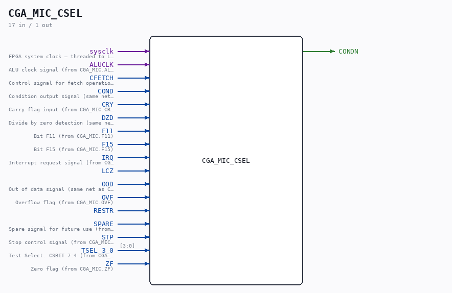
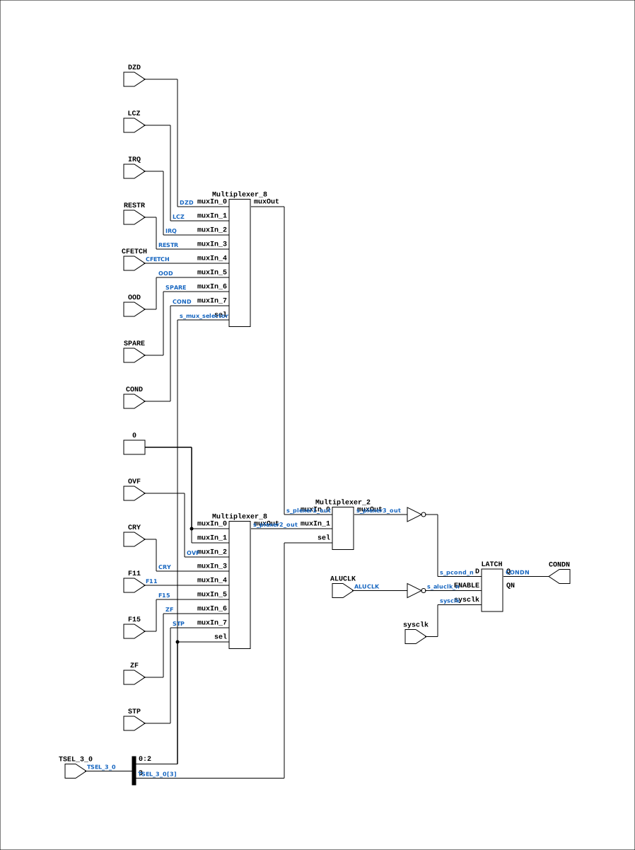
Schematic
Drawn from the Verilog: the yosys netlist of the Simulation (Verilator) build, instance CORE.CPU_BOARD.CPU.PROC.CGA.DELILAH.MIC.CSEL. Sub-modules are boxes (click the picture to open it full size; there every sub-module box links to its page, and every wire shows its Verilog name).
Description
ND120 CGA (CPU Gate Array / DELILAH) /CGA/MIC/CSEL CONDITION SELECT Page 14 SHEET 1 of 1 Last reviewed: 10-NOV-2024 Ronny Hansen
Ports
| Direction | Width | Name | Description |
|---|---|---|---|
| input | 1 |
sysclk |
FPGA system clock — threaded to LATCH |
| input | 1 |
ALUCLK |
ALU clock signal (from CGA_MIC.ALUCLK) |
| input | 1 |
CFETCH |
Control signal for fetch operation (from CGA_MIC.CFETCH) |
| input | 1 |
COND |
Condition output signal (same net as CGA_MIC.COND) |
| input | 1 |
CRY |
Carry flag input (from CGA_MIC.CRY) |
| input | 1 |
DZD |
Divide by zero detection (same net as CGA_MIC.DZD) |
| input | 1 |
F11 |
Bit F11 (from CGA_MIC.F11) |
| input | 1 |
F15 |
Bit F15 (from CGA_MIC.F15) |
| input | 1 |
IRQ |
Interrupt request signal (from CGA_MIC.IRQ) |
| input | 1 |
LCZ |
|
| input | 1 |
OOD |
Out of data signal (same net as CGA_MIC.OOD) |
| input | 1 |
OVF |
Overflow flag (from CGA_MIC.OVF) |
| input | 1 |
RESTR |
|
| input | 1 |
SPARE |
Spare signal for future use (from CGA_MIC.SPARE) |
| input | 1 |
STP |
Stop control signal (from CGA_MIC.STP) |
| input | [3:0] |
TSEL_3_0 |
Test Select. CSBIT 7:4 (from CGA_MIC_CONDREG.TSEL_3_0) |
| input | 1 |
ZF |
Zero flag (from CGA_MIC.ZF) |
| output | 1 |
CONDN |
Verilog source
Verilog/DELILAH-CPU/CGA_MIC/circuit/CGA_MIC_CSEL.v on GitHub.
Show the Verilog of CGA_MIC_CSEL (170 lines)
/**************************************************************************
** ND120 CGA (CPU Gate Array / DELILAH)                                  **
** /CGA/MIC/CSEL                                                         **
** CONDITION SELECT                                                      **
**                                                                       **
** Page 14                                                               **
** SHEET 1 of 1                                                          **
**                                                                       **
** Last reviewed: 10-NOV-2024                                            **
** Ronny Hansen                                                          **
***************************************************************************/

module CGA_MIC_CSEL (
    input       sysclk,    //! FPGA system clock — threaded to LATCH
    input       ALUCLK,    //! ALU clock signal (from CGA_MIC.ALUCLK)
    input       CFETCH,    //! Control signal for fetch operation (from CGA_MIC.CFETCH)
    input       COND,      //! Condition output signal (same net as CGA_MIC.COND)
    input       CRY,       //! Carry flag input (from CGA_MIC.CRY)
    input       DZD,       //! Divide by zero detection (same net as CGA_MIC.DZD)
    input       F11,       //! Bit F11 (from CGA_MIC.F11)
    input       F15,       //! Bit F15 (from CGA_MIC.F15)
    input       IRQ,       //! Interrupt request signal (from CGA_MIC.IRQ)
    input       LCZ,
    input       OOD,       //! Out of data signal (same net as CGA_MIC.OOD)
    input       OVF,       //! Overflow flag (from CGA_MIC.OVF)
    input       RESTR,
    input       SPARE,     //! Spare signal for future use (from CGA_MIC.SPARE)
    input       STP,       //! Stop control signal (from CGA_MIC.STP)
    input [3:0] TSEL_3_0,  //! Test Select. CSBIT 7:4 (from CGA_MIC_CONDREG.TSEL_3_0)
    input       ZF,        //! Zero flag (from CGA_MIC.ZF)

    output CONDN
);

  /*******************************************************************************
   ** The wires are defined here                                                 **
   *******************************************************************************/
  wire [2:0] s_mux_selector;
  wire [3:0] s_tsel_3_0;
  wire       s_aluclk_n;
  (* mark_debug = "true", DONT_TOUCH = "true" *) wire       s_aluclk;
  wire       s_cfetch_n;
  (* mark_debug = "true", DONT_TOUCH = "true" *) wire       s_cond_n_out;
  wire       s_cond;
  wire       s_cry;
  wire       s_dzd;
  wire       s_F11;
  wire       s_f15;
  wire       s_gnd;
  wire       s_irq;
  wire       s_lcz;
  wire       s_ood;
  wire       s_ovf;
  (* mark_debug = "true", DONT_TOUCH = "true" *) wire       s_pcond_n;
  wire       s_plexer1_out;
  wire       s_plexer2_out;
  wire       s_plexer3_out;
  wire       s_restr;
  wire       s_spare;
  wire       s_stp;
  wire       s_tsel_0;
  wire       s_tsel_1;
  wire       s_tsel_2;
  wire       s_zf;

  /*******************************************************************************
   ** Here all wiring is defined                                                 **
   *******************************************************************************/
  assign s_mux_selector[0] = s_tsel_0;
  assign s_mux_selector[1] = s_tsel_1;
  assign s_mux_selector[2] = s_tsel_2;
  assign s_tsel_0         = s_tsel_3_0[0];
  assign s_tsel_1         = s_tsel_3_0[1];
  assign s_tsel_2         = s_tsel_3_0[2];

  /*******************************************************************************
   ** Here all input connections are defined                                     **
   *******************************************************************************/
  assign s_aluclk         = ALUCLK;
  assign s_cfetch_n       = CFETCH;
  assign s_cond           = COND;
  assign s_cry            = CRY;
  assign s_dzd            = DZD;
  assign s_F11            = F11;
  assign s_f15            = F15;
  assign s_irq            = IRQ;
  assign s_lcz            = LCZ;
  assign s_ood            = OOD;
  assign s_ovf            = OVF;
  assign s_restr          = RESTR;
  assign s_spare          = SPARE;
  assign s_stp            = STP;
  assign s_tsel_3_0[3:0]  = TSEL_3_0;
  assign s_zf             = ZF;

  /*******************************************************************************
   ** Here all output connections are defined                                    **
   *******************************************************************************/
  assign CONDN            = s_cond_n_out;

  /*******************************************************************************
   ** Here all in-lined components are defined                                   **
   *******************************************************************************/

  // Ground
  assign s_gnd   = 1'b0;


  // NOT Gate
  assign s_pcond_n   = ~s_plexer3_out;

  // NOT Gate
  assign s_aluclk_n    = ~s_aluclk;

  /*******************************************************************************
   ** Here all normal components are defined                                     **
   *******************************************************************************/
  Multiplexer_8 PLEXERS_1 (
      .muxIn_0(s_dzd),
      .muxIn_1(s_lcz),
      .muxIn_2(s_irq),
      .muxIn_3(s_restr),
      .muxIn_4(s_cfetch_n),
      .muxIn_5(s_ood),
      .muxIn_6(s_spare),
      .muxIn_7(s_cond),
      .muxOut(s_plexer1_out),
      .sel(s_mux_selector[2:0])
  );

  Multiplexer_8 PLEXERS_2 (
      .muxIn_0(s_gnd),
      .muxIn_1(s_gnd),
      .muxIn_2(s_ovf),
      .muxIn_3(s_cry),
      .muxIn_4(s_F11),
      .muxIn_5(s_f15),
      .muxIn_6(s_zf),
      .muxIn_7(s_stp),
      .muxOut(s_plexer2_out),
      .sel(s_mux_selector[2:0])
  );

  Multiplexer_2 PLEXERS_3 (
      .muxIn_0(s_plexer1_out),
      .muxIn_1(s_plexer2_out),
      .muxOut(s_plexer3_out),
      .sel(s_tsel_3_0[3])
  );


  /*******************************************************************************
   ** Here all sub-circuits are defined                                          **
   *******************************************************************************/

  // QUARTUS_LATCH_RENAME: see the header comment in Shared/ndlib/LATCH.v -
  // Quartus's built-in LATCH primitive collides with this module's name.
`ifdef QUARTUS_LATCH_RENAME
  ND120_LATCH CSEL_LATCH (
`else
  LATCH CSEL_LATCH (
`endif
      .sysclk(sysclk),
      .D(s_pcond_n),
      .ENABLE(s_aluclk_n),
      .Q(s_cond_n_out),
      .QN()
  );

endmodule