CGA_CPU_ALU_RALU
Source: Verilog/DELILAH-CPU/CGA_ALU/circuit/CGA_CPU_ALU_RALU.v
Where it sits (Simulation): ND120_TOP > ND120_CORE > ND3202D > CPU_15 > CPU_PROC_32 > CPU_PROC_CGA_33 > CGA > CGA_ALU > CGA_CPU_ALU_RALU
- instance path: CORE.CPU_BOARD.CPU.PROC.CGA.DELILAH.ALU.ALU_RALU
Used in: CGA_ALU (all tops)
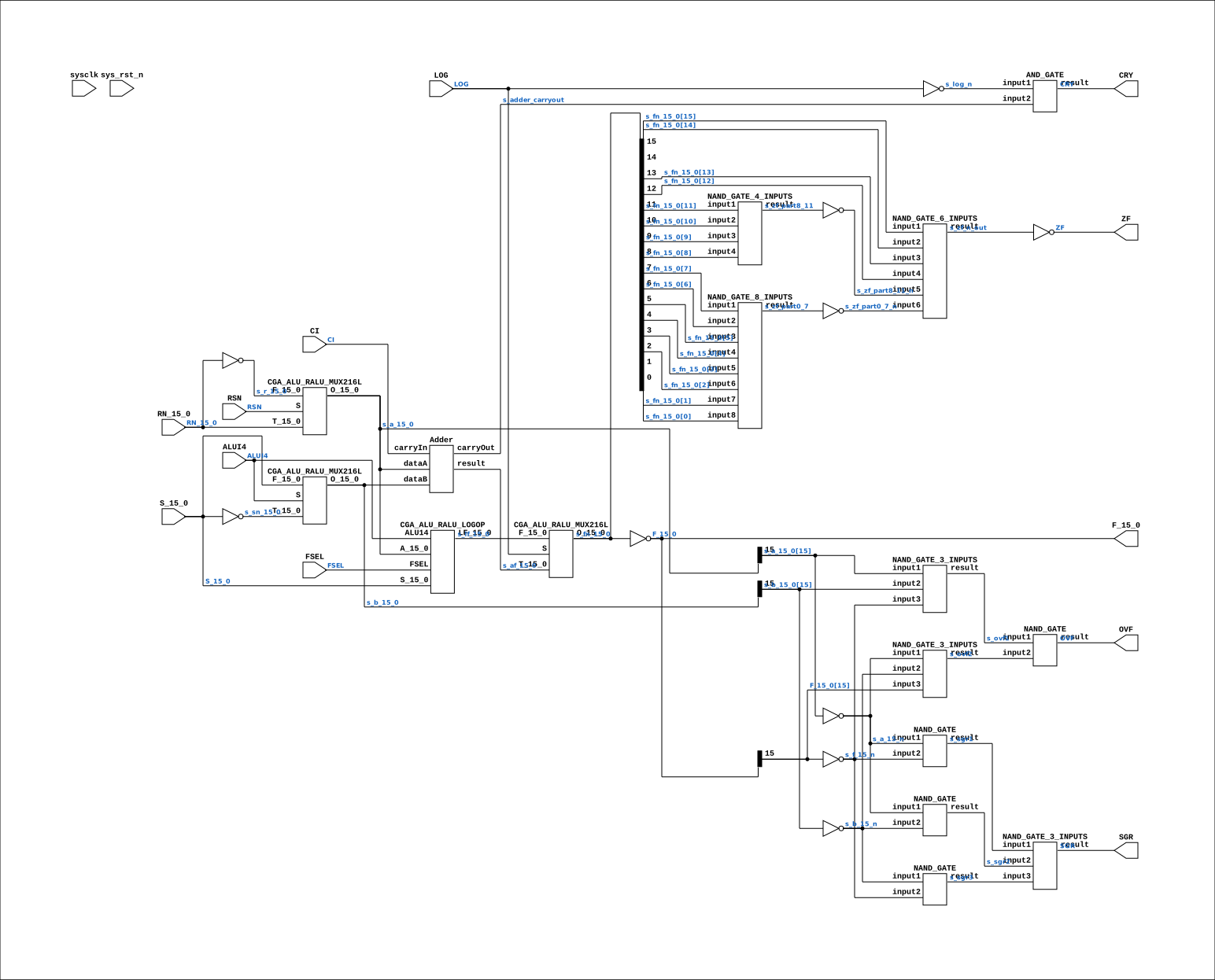
Contains: Adder, AND_GATE, CGA_ALU_RALU_LOGOP, CGA_ALU_RALU_MUX216L x3, NAND_GATE x4, NAND_GATE_3_INPUTS x3, NAND_GATE_4_INPUTS, NAND_GATE_6_INPUTS, NAND_GATE_8_INPUTS
Module hierarchy - All modules
Schematic
Drawn from the Verilog: the yosys netlist of the Simulation (Verilator) build, instance CORE.CPU_BOARD.CPU.PROC.CGA.DELILAH.ALU.ALU_RALU. Sub-modules are boxes (click the picture to open it full size; there every sub-module box links to its page, and every wire shows its Verilog name).
Description
ND120 CGA (CPU Gate Array / DELILAH) /CGA/ALU/RALU RALU Page 46 SHEET 1 of 1 Last reviewed: 20-DEC-2024 Ronny Hansen
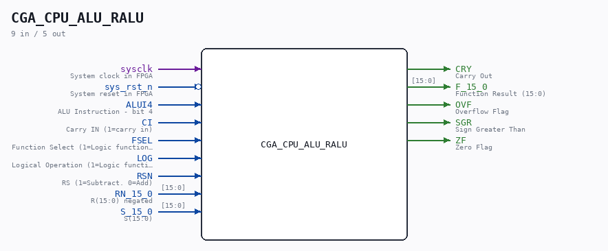
Ports
| Direction | Width | Name | Description |
|---|---|---|---|
| input | 1 |
sysclk |
System clock in FPGA |
| input | 1 |
sys_rst_n (active low) |
System reset in FPGA |
| input | 1 |
ALUI4 |
ALU Instruction - bit 4 |
| input | 1 |
CI |
Carry IN (1=carry in) |
| input | 1 |
FSEL |
Function Select (1=Logic function (XOR), 0=OR/AND/NOT) |
| input | 1 |
LOG |
Logical Operation (1=Logic function (AND/OR). 0=ADD/SUB) |
| input | 1 |
RSN |
RS (1=Subtract. 0=Add) |
| input | [15:0] |
RN_15_0 |
R(15:0) negated |
| input | [15:0] |
S_15_0 |
S(15:0) |
| output | 1 |
CRY |
Carry Out |
| output | [15:0] |
F_15_0 |
Function Result (15:0) |
| output | 1 |
OVF |
Overflow Flag |
| output | 1 |
SGR |
Sign Greater Than |
| output | 1 |
ZF |
Zero Flag |
Verilog source
Verilog/DELILAH-CPU/CGA_ALU/circuit/CGA_CPU_ALU_RALU.v on GitHub.
Show the Verilog of CGA_CPU_ALU_RALU (257 lines)
/**************************************************************************
** ND120 CGA (CPU Gate Array / DELILAH)                                  **
** /CGA/ALU/RALU                                                         **
** RALU                                                                  **
**                                                                       **
** Page 46                                                               **
** SHEET 1 of 1                                                          **
**                                                                       **
** Last reviewed: 20-DEC-2024                                            **
** Ronny Hansen                                                          **
**************************************************************************/

module CGA_CPU_ALU_RALU (
    input sysclk,    // System clock in FPGA
    input sys_rst_n, // System reset in FPGA

    input        ALUI4,    //! ALU Instruction - bit 4
    input        CI,       //! Carry IN (1=carry in)
    input        FSEL,     //! Function Select (1=Logic function (XOR), 0=OR/AND/NOT)
    input        LOG,      //! Logical Operation (1=Logic function (AND/OR). 0=ADD/SUB)
    input        RSN,      //! RS (1=Subtract. 0=Add)
    input [15:0] RN_15_0,  //! R(15:0) negated
    input [15:0] S_15_0,   //! S(15:0)

    output        CRY,     //! Carry Out
    output [15:0] F_15_0,  //! Function Result (15:0)
    output        OVF,     //! Overflow Flag
    output        SGR,     //! Sign Greater Than
    output        ZF       //! Zero Flag
);

  /*******************************************************************************
   ** The wires are defined here                                                 **
   *******************************************************************************/
  wire [15:0] s_a_15_0;
  wire [15:0] s_s_15_0;
  wire [15:0] s_rn_15_0;
  wire [15:0] s_fn_15_0;
  wire [15:0] s_b_15_0;
  wire [15:0] s_lf_15_0;
  wire [15:0] s_af_15_0;
  wire [15:0] s_f_15_0_out;
  wire [15:0] s_sn_15_0;
  wire [15:0] s_r_15_0;
  wire        s_a_15_n;
  wire        s_adder_carryout;
  wire        s_alui4;
  wire        s_b_15_n;
  wire        s_ci;
  wire        s_cry_out;
  wire        s_f_15_n;
  wire        s_fsel;
  wire        s_log_n;
  wire        s_log;
  wire        s_ovf_out;
  wire        s_ovf1;
  wire        s_ovf2;
  wire        s_rs_n;
  wire        s_sgr_out;
  wire        s_sgr1;
  wire        s_sgr2;
  wire        s_sgr3;
  wire        s_zf_n_out;
  wire        s_zf_out;
  wire        s_zf_part0_7_n;
  wire        s_zf_part0_7;
  wire        s_zf_part8_11_n;
  wire        s_zf_part8_11;

  /*******************************************************************************
   ** Here all input connections are defined                                     **
   *******************************************************************************/
  assign s_s_15_0[15:0]     = S_15_0;
  assign s_rn_15_0[15:0]    = RN_15_0;
  assign s_fsel             = FSEL;
  assign s_alui4            = ALUI4;
  assign s_log              = LOG;
  assign s_rs_n             = RSN;
  assign s_ci               = CI;

  /*******************************************************************************
   ** Here all output connections are defined                                    **
   *******************************************************************************/
  assign CRY                = s_cry_out;
  assign F_15_0             = s_f_15_0_out[15:0];
  assign OVF                = s_ovf_out;
  assign SGR                = s_sgr_out;
  assign ZF                 = s_zf_out;

  /*******************************************************************************
   ** Here all in-lined components are defined                                   **
   *******************************************************************************/

  // NOT Gate
  assign s_a_15_n           = ~s_a_15_0[15];
  assign s_b_15_n           = ~s_b_15_0[15];
  assign s_f_15_n           = ~s_f_15_0_out[15];
  assign s_f_15_0_out[15:0] = ~s_fn_15_0[15:0];
  assign s_log_n            = ~s_log;
  assign s_r_15_0           = ~s_rn_15_0;
  assign s_sn_15_0          = ~s_s_15_0;
  assign s_zf_out           = ~s_zf_n_out;
  assign s_zf_part0_7_n     = ~s_zf_part0_7;
  assign s_zf_part8_11_n    = ~s_zf_part8_11;

  /*******************************************************************************
   ** Here all normal components are defined                                     **
   *******************************************************************************/
  NAND_GATE #(
      .BubblesMask(2'b00)
  ) GATES_1 (
      .input1(s_a_15_n),
      .input2(s_f_15_n),
      .result(s_sgr1)
  );

  NAND_GATE #(
      .BubblesMask(2'b00)
  ) GATES_2 (
      .input1(s_a_15_n),
      .input2(s_b_15_n),
      .result(s_sgr2)
  );

  NAND_GATE #(
      .BubblesMask(2'b00)
  ) GATES_3 (
      .input1(s_b_15_n),
      .input2(s_f_15_n),
      .result(s_sgr3)
  );

  NAND_GATE_3_INPUTS #(
      .BubblesMask(3'b000)
  ) GATES_4 (
      .input1(s_a_15_0[15]),
      .input2(s_b_15_0[15]),
      .input3(s_f_15_n),
      .result(s_ovf1)
  );

  NAND_GATE_3_INPUTS #(
      .BubblesMask(3'b000)
  ) GATES_5 (
      .input1(s_a_15_n),
      .input2(s_b_15_n),
      .input3(s_f_15_0_out[15]),
      .result(s_ovf2)
  );

  NAND_GATE_4_INPUTS #(
      .BubblesMask(4'h0)
  ) GATES_6 (
      .input1(s_fn_15_0[11]),
      .input2(s_fn_15_0[10]),
      .input3(s_fn_15_0[9]),
      .input4(s_fn_15_0[8]),
      .result(s_zf_part8_11)
  );

  NAND_GATE_8_INPUTS #(
      .BubblesMask(8'h00)
  ) GATES_7 (
      .input1(s_fn_15_0[7]),
      .input2(s_fn_15_0[6]),
      .input3(s_fn_15_0[5]),
      .input4(s_fn_15_0[4]),
      .input5(s_fn_15_0[3]),
      .input6(s_fn_15_0[2]),
      .input7(s_fn_15_0[1]),
      .input8(s_fn_15_0[0]),
      .result(s_zf_part0_7)
  );

  AND_GATE #(
      .BubblesMask(2'b00)
  ) GATES_8 (
      .input1(s_log_n),
      .input2(s_adder_carryout),
      .result(s_cry_out)
  );

  NAND_GATE_3_INPUTS #(
      .BubblesMask(3'b000)
  ) GATES_9 (
      .input1(s_sgr1),
      .input2(s_sgr2),
      .input3(s_sgr3),
      .result(s_sgr_out)
  );

  NAND_GATE #(
      .BubblesMask(2'b00)
  ) GATES_10 (
      .input1(s_ovf1),
      .input2(s_ovf2),
      .result(s_ovf_out)
  );

  NAND_GATE_6_INPUTS #(
      .BubblesMask({2'b00, 4'h0})
  ) GATES_11 (
      .input1(s_fn_15_0[15]),
      .input2(s_fn_15_0[14]),
      .input3(s_fn_15_0[13]),
      .input4(s_fn_15_0[12]),
      .input5(s_zf_part8_11_n),
      .input6(s_zf_part0_7_n),
      .result(s_zf_n_out)
  );

  Adder #(
      .extendedBits(17),
      .nrOfBits(16)
  ) ARITH_12 (
      .carryIn(s_ci),
      .carryOut(s_adder_carryout),
      .dataA(s_a_15_0[15:0]),
      .dataB(s_b_15_0[15:0]),
      .result(s_af_15_0[15:0])
  );


  /*******************************************************************************
   ** Here all sub-circuits are defined                                          **
   *******************************************************************************/

  CGA_ALU_RALU_MUX216L RN_R_MUX (
      .S(s_rs_n),
      .F_15_0(s_r_15_0[15:0]),
      .T_15_0(s_rn_15_0[15:0]),
      .O_15_0(s_a_15_0[15:0])  // out
  );

  CGA_ALU_RALU_MUX216L SN_S_MUX (
      .S(s_alui4),
      .F_15_0(s_s_15_0[15:0]),
      .T_15_0(s_sn_15_0[15:0]),
      .O_15_0(s_b_15_0[15:0])  // out
  );

  CGA_ALU_RALU_LOGOP LOGOP (
      .ALU14(s_alui4),
      .FSEL(s_fsel),
      .A_15_0(s_a_15_0[15:0]),
      .S_15_0(s_s_15_0[15:0]),
      .LF_15_0(s_lf_15_0[15:0])  // out
  );

  CGA_ALU_RALU_MUX216L AF_LF_MUX (
      .S(s_log),
      .F_15_0(s_lf_15_0[15:0]),
      .T_15_0(s_af_15_0[15:0]),
      .O_15_0(s_fn_15_0[15:0])  // out
  );

endmodule