CGA_WRF
CPU internal 'Register File' - Read and Write operations on 16 registers
Source: Verilog/DELILAH-CPU/CGA_WRF/circuit/CGA_WRF.v
· Author: Ronny Hansen
Where it sits (Simulation): ND120_TOP > ND120_CORE > ND3202D > CPU_15 > CPU_PROC_32 > CPU_PROC_CGA_33 > CGA > CGA_WRF
- instance path: CORE.CPU_BOARD.CPU.PROC.CGA.DELILAH.WRF
Used in: CGA (all tops)
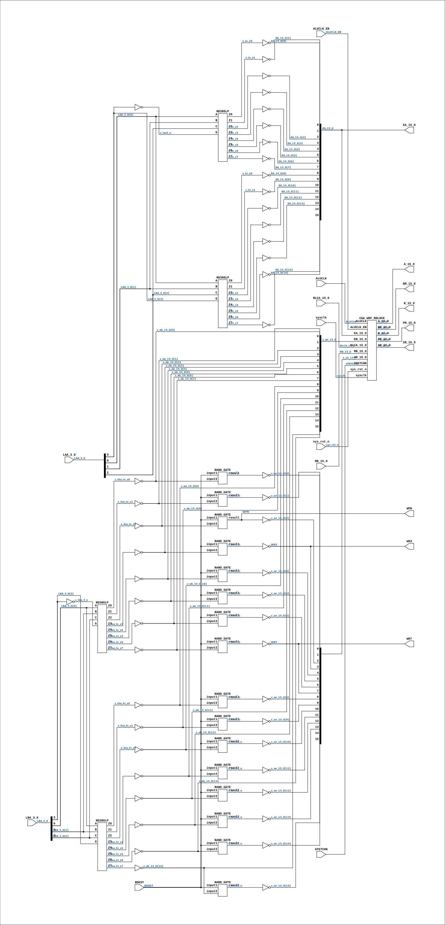
Contains: CGA_WRF_RBLOCK, NAND_GATE x16, ND38GLP x4
Module hierarchy - All modules
Schematic
Drawn from the Verilog: the yosys netlist of the Simulation (Verilator) build, instance CORE.CPU_BOARD.CPU.PROC.CGA.DELILAH.WRF. Sub-modules are boxes (click the picture to open it full size; there every sub-module box links to its page, and every wire shows its Verilog name).
Description
ND120 CPU, MM&M CGA/WRF WRF: Working Register File (PDF page 59) Last reviewed: 9-FEB-2025 Ronny Hansen
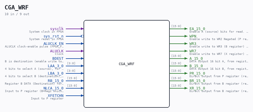
Ports
| Direction | Width | Name | Description |
|---|---|---|---|
| input | 1 |
sysclk |
System clock in FPGA |
| input | 1 |
sys_rst_n (active low) |
System reset in FPGA |
| input | 1 |
ALUCLK_EN |
ALUCLK clock-enable pulse (FPGA_FF_MODE, else 0) |
| input | 1 |
ALUCLK |
Clock |
| input | 1 |
BDEST |
B is destination (enable write to B from 'RB_15_0' on ALUCLK) |
| input | [3:0] |
LAA_3_0 |
4 bits to select A (source), for 16 different registers. |
| input | [3:0] |
LBA_3_0 |
4 bits to select B (destination), for 16 different registers. |
| input | [15:0] |
RB_15_0 |
Register B DATA (Destination) for WRITE. 16 bits to select register(s) |
| input | [15:0] |
NLCA_15_0 |
Input to P register (B=Reg2 which is P) |
| input | 1 |
XFETCHN |
Input to P register |
| output | [15:0] |
EA_15_0 |
Enable A (source) bits for read. 16 bits to select register. |
| output | 1 |
WPN |
Enable write to WR2 Negated (P register) (from WR_15_0) |
| output | 1 |
WR3 |
Enable write to WR3 (B register) (from WR_15_0) |
| output | 1 |
WR7 |
Enable write to WR7 (X register) (from WR_15_0) |
| output | [15:0] |
A_15_0 |
DATA output 16 bit A, from register selected by LAA_3_0 |
| output | [15:0] |
B_15_0 |
DATA output 16 bit B, from register selected by LBA_3_0 |
| output | [15:0] |
PR_15_0 |
Direct output from P register (register #2) |
| output | [15:0] |
BR_15_0 |
Direct output from B register (register #3) |
| output | [15:0] |
XR_15_0 |
Direct output from B register (register #7) |
Verilog source
Verilog/DELILAH-CPU/CGA_WRF/circuit/CGA_WRF.v on GitHub.
Show the Verilog of CGA_WRF (544 lines)
/**************************************************************************
** ND120 CPU, MM&M                                                       **
** CGA/WRF                                                               **
** WRF: Working Register File                                            **
** (PDF page 59)                                                         **
**                                                                       **
** Last reviewed: 9-FEB-2025                                             **
** Ronny Hansen                                                          **
***************************************************************************/


//! @title CPU internal 'Register File' - Read and Write operations on 16 registers
//! @author Ronny Hansen

//! Register 0 (Z),
//! Register 1 (D),
//! Register 2 (P),
//! Register 3 (B),
//! Register 4 (L),
//! Register 5 (A),
//! Register 6 (T),
//! Register 7 (X),
//! Register 8 (STS),
//! (internal registers)
//! Register 9 (R1),
//! Register 10 (R2),
//! Register 11 (R3),
//! Register 12 (R4),
//! Register 13 (R5),
//! Register 14 (R6),
//! Register 15 (R7)

module CGA_WRF (
    // System input signals
    input sysclk,    // System clock in FPGA
    input sys_rst_n, // System reset in FPGA


    // Input signals
    input       ALUCLK_EN,  //! ALUCLK clock-enable pulse (FPGA_FF_MODE, else 0)
    input       ALUCLK,   //! Clock
    input       BDEST,    //! B is destination (enable write to B from 'RB_15_0' on ALUCLK)
    input [3:0] LAA_3_0,  //! 4 bits to select A (source), for 16 different registers.
    input [3:0] LBA_3_0,  //! 4 bits to select B (destination), for 16 different registers.

    input [15:0] RB_15_0,    //! Register B DATA (Destination) for WRITE. 16 bits to select register(s)

    input [15:0] NLCA_15_0,  //! Input to P register (B=Reg2 which is P)
    input        XFETCHN,    //! Input to P register


    // Output signals
    output [15:0] EA_15_0,  //! Enable A (source) bits for read. 16 bits to select register.

    output WPN,  //! Enable write to WR2 Negated (P register) (from WR_15_0)
    output WR3,  //! Enable write to WR3 (B register) (from WR_15_0)
    output WR7,  //! Enable write to WR7 (X register) (from WR_15_0)


    output [15:0] A_15_0,  //! DATA output 16 bit A, from register selected by LAA_3_0
    output [15:0] B_15_0,  //! DATA output 16 bit B, from register selected by LBA_3_0

    output [15:0] PR_15_0,  //! Direct output from P register (register #2)
    output [15:0] BR_15_0,  //! Direct output from B register (register #3)
    output [15:0] XR_15_0   //! Direct output from B register (register #7)


);


  /*******************************************************************************
   ** The wires are defined here                                                 **
   *******************************************************************************/
  wire        s_aluclk;
  wire        s_bdest;
  wire        s_hi_z0;
  wire        s_hi_z1;
  wire        s_hi_z2;
  wire        s_hi_z3;
  wire        s_hi_z4;
  wire        s_hi_z5;
  wire        s_hi_z6;
  wire        s_hi_z7;
  wire        s_laa3_n;
  wire        s_lba_3_n;
  wire        s_lba_hi_z0;
  wire        s_lba_hi_z1;
  wire        s_lba_hi_z2;
  wire        s_lba_hi_z3;
  wire        s_lba_hi_z4;
  wire        s_lba_hi_z5;
  wire        s_lba_hi_z6;
  wire        s_lba_hi_z7;
  wire        s_lba_lo_z0;
  wire        s_lba_lo_z1;
  wire        s_lba_lo_z2;
  wire        s_lba_lo_z3;
  wire        s_lba_lo_z4;
  wire        s_lba_lo_z5;
  wire        s_lba_lo_z6;
  wire        s_lba_lo_z7;
  wire        s_lo_z0;
  wire        s_lo_z1;
  wire        s_lo_z2;
  wire        s_lo_z3;
  wire        s_lo_z4;
  wire        s_lo_z5;
  wire        s_lo_z6;
  wire        s_lo_z7;
  wire        s_wp_n;
  wire        s_wr_1_n;
  wire        s_wr_10_n;
  wire        s_wr_11_n;
  wire        s_wr_12_n;
  wire        s_wr_13_n;
  wire        s_wr_14_n;
  wire        s_wr_15_n;
  wire        s_wr_3_n;
  wire        s_wr_4_n;
  wire        s_wr_5_n;
  wire        s_wr_6_n;
  wire        s_wr_7_n;
  wire        s_wr_8_n;
  wire        s_wr_9_n;
  wire        s_wr0_n;
  wire        s_xfetch_n;
  wire [ 3:0] s_laa_3_0;
  wire [ 3:0] s_lba_3_0;
  wire [15:0] s_a_15_0_out;
  wire [15:0] s_b_15_0_out;
  wire [15:0] s_br_15_0_out;
  wire [15:0] s_ea_15_0_out;
  wire [15:0] s_eb_15_0;
  wire [15:0] s_nlca_15_0;
  wire [15:0] s_pr_15_0_out;
  wire [15:0] s_rb_15_0;
  wire [15:0] s_wr_15_0;
  wire [15:0] s_xr_15_0_out;


  /*******************************************************************************
   ** The module functionality is described here                                 **
   *******************************************************************************/

  /*******************************************************************************
   ** Here all input connections are defined                                     **
   *******************************************************************************/
  assign s_nlca_15_0[15:0] = NLCA_15_0;
  assign s_laa_3_0[3:0]    = LAA_3_0;
  assign s_lba_3_0[3:0]    = LBA_3_0;
  assign s_rb_15_0[15:0]   = RB_15_0;
  assign s_bdest           = BDEST;
  assign s_aluclk          = ALUCLK;
  assign s_xfetch_n        = XFETCHN;

  /*******************************************************************************
   ** Here all output connections are defined                                    **
   *******************************************************************************/
  assign A_15_0            = s_a_15_0_out[15:0];
  assign BR_15_0           = s_br_15_0_out[15:0];
  assign B_15_0            = s_b_15_0_out[15:0];
  assign EA_15_0           = s_ea_15_0_out[15:0];
  assign PR_15_0           = s_pr_15_0_out[15:0];
  assign WPN               = s_wp_n;
  assign WR3               = s_wr_15_0[3];
  assign WR7               = s_wr_15_0[7];
  assign XR_15_0           = s_xr_15_0_out[15:0];

  /*******************************************************************************
   ** Here all in-lined components are defined                                   **
   *******************************************************************************/

  // NOT Gate
  assign s_wr_15_0[0]      = ~s_wr0_n;

  // NOT Gate
  assign s_wr_15_0[1]      = ~s_wr_1_n;

  // NOT Gate
  assign s_wr_15_0[2]      = ~s_wp_n;

  // NOT Gate
  assign s_wr_15_0[3]      = ~s_wr_3_n;

  // NOT Gate
  assign s_wr_15_0[4]      = ~s_wr_4_n;

  // NOT Gate
  assign s_wr_15_0[5]      = ~s_wr_5_n;

  // NOT Gate
  assign s_wr_15_0[6]      = ~s_wr_6_n;

  // NOT Gate
  assign s_wr_15_0[7]      = ~s_wr_7_n;

  // NOT Gate
  assign s_wr_15_0[8]      = ~s_wr_8_n;

  // NOT Gate
  assign s_wr_15_0[9]      = ~s_wr_9_n;

  // NOT Gate
  assign s_wr_15_0[10]     = ~s_wr_10_n;

  // NOT Gate
  assign s_wr_15_0[11]     = ~s_wr_11_n;

  // NOT Gate
  assign s_wr_15_0[12]     = ~s_wr_12_n;

  // NOT Gate
  assign s_wr_15_0[13]     = ~s_wr_13_n;

  // NOT Gate
  assign s_wr_15_0[14]     = ~s_wr_14_n;

  // NOT Gate
  assign s_wr_15_0[15]     = ~s_wr_15_n;

  // NOT Gate
  assign s_laa3_n          = ~s_laa_3_0[3];

  // NOT Gate
  assign s_lba_3_n         = ~s_lba_3_0[3];

  // NOT Gate
  assign s_eb_15_0[8]      = ~s_lba_hi_z0;

  // NOT Gate
  assign s_eb_15_0[9]      = ~s_lba_hi_z1;

  // NOT Gate
  assign s_eb_15_0[10]     = ~s_lba_hi_z2;

  // NOT Gate
  assign s_eb_15_0[11]     = ~s_lba_hi_z3;

  // NOT Gate
  assign s_eb_15_0[12]     = ~s_lba_hi_z4;

  // NOT Gate
  assign s_eb_15_0[13]     = ~s_lba_hi_z5;

  // NOT Gate
  assign s_eb_15_0[14]     = ~s_lba_hi_z6;

  // NOT Gate
  assign s_eb_15_0[15]     = ~s_lba_hi_z7;

  // NOT Gate
  assign s_ea_15_0_out[0]  = ~s_lo_z0;

  // NOT Gate
  assign s_ea_15_0_out[1]  = ~s_lo_z1;

  // NOT Gate
  assign s_ea_15_0_out[2]  = ~s_lo_z2;

  // NOT Gate
  assign s_ea_15_0_out[3]  = ~s_lo_z3;

  // NOT Gate
  assign s_ea_15_0_out[4]  = ~s_lo_z4;

  // NOT Gate
  assign s_ea_15_0_out[5]  = ~s_lo_z5;

  // NOT Gate
  assign s_ea_15_0_out[6]  = ~s_lo_z6;

  // NOT Gate
  assign s_ea_15_0_out[7]  = ~s_lo_z7;

  // NOT Gate
  assign s_ea_15_0_out[8]  = ~s_hi_z0;

  // NOT Gate
  assign s_ea_15_0_out[9]  = ~s_hi_z1;

  // NOT Gate
  assign s_ea_15_0_out[10] = ~s_hi_z2;

  // NOT Gate
  assign s_ea_15_0_out[11] = ~s_hi_z3;

  // NOT Gate
  assign s_ea_15_0_out[12] = ~s_hi_z4;

  // NOT Gate
  assign s_ea_15_0_out[13] = ~s_hi_z5;

  // NOT Gate
  assign s_ea_15_0_out[14] = ~s_hi_z6;

  // NOT Gate
  assign s_ea_15_0_out[15] = ~s_hi_z7;

  // NOT Gate
  assign s_eb_15_0[0]      = ~s_lba_lo_z0;

  // NOT Gate
  assign s_eb_15_0[1]      = ~s_lba_lo_z1;

  // NOT Gate
  assign s_eb_15_0[2]      = ~s_lba_lo_z2;

  // NOT Gate
  assign s_eb_15_0[3]      = ~s_lba_lo_z3;

  // NOT Gate
  assign s_eb_15_0[4]      = ~s_lba_lo_z4;

  // NOT Gate
  assign s_eb_15_0[5]      = ~s_lba_lo_z5;

  // NOT Gate
  assign s_eb_15_0[6]      = ~s_lba_lo_z6;

  // NOT Gate
  assign s_eb_15_0[7]      = ~s_lba_lo_z7;

  /*******************************************************************************
   ** Here all normal components are defined                                     **
   *******************************************************************************/
  NAND_GATE #(
      .BubblesMask(2'b00)
  ) GATES_1 (
      .input1(s_bdest),
      .input2(s_eb_15_0[0]),
      .result(s_wr0_n)
  );

  NAND_GATE #(
      .BubblesMask(2'b00)
  ) GATES_2 (
      .input1(s_bdest),
      .input2(s_eb_15_0[1]),
      .result(s_wr_1_n)
  );

  NAND_GATE #(
      .BubblesMask(2'b00)
  ) GATES_3 (
      .input1(s_bdest),
      .input2(s_eb_15_0[2]),
      .result(s_wp_n)
  );

  NAND_GATE #(
      .BubblesMask(2'b00)
  ) GATES_4 (
      .input1(s_bdest),
      .input2(s_eb_15_0[3]),
      .result(s_wr_3_n)
  );

  NAND_GATE #(
      .BubblesMask(2'b00)
  ) GATES_5 (
      .input1(s_bdest),
      .input2(s_eb_15_0[4]),
      .result(s_wr_4_n)
  );

  NAND_GATE #(
      .BubblesMask(2'b00)
  ) GATES_6 (
      .input1(s_bdest),
      .input2(s_eb_15_0[5]),
      .result(s_wr_5_n)
  );

  NAND_GATE #(
      .BubblesMask(2'b00)
  ) GATES_7 (
      .input1(s_bdest),
      .input2(s_eb_15_0[6]),
      .result(s_wr_6_n)
  );

  NAND_GATE #(
      .BubblesMask(2'b00)
  ) GATES_8 (
      .input1(s_bdest),
      .input2(s_eb_15_0[7]),
      .result(s_wr_7_n)
  );

  NAND_GATE #(
      .BubblesMask(2'b00)
  ) GATES_9 (
      .input1(s_bdest),
      .input2(s_eb_15_0[8]),
      .result(s_wr_8_n)
  );

  NAND_GATE #(
      .BubblesMask(2'b00)
  ) GATES_10 (
      .input1(s_bdest),
      .input2(s_eb_15_0[9]),
      .result(s_wr_9_n)
  );

  NAND_GATE #(
      .BubblesMask(2'b00)
  ) GATES_11 (
      .input1(s_bdest),
      .input2(s_eb_15_0[10]),
      .result(s_wr_10_n)
  );

  NAND_GATE #(
      .BubblesMask(2'b00)
  ) GATES_12 (
      .input1(s_bdest),
      .input2(s_eb_15_0[11]),
      .result(s_wr_11_n)
  );

  NAND_GATE #(
      .BubblesMask(2'b00)
  ) GATES_13 (
      .input1(s_bdest),
      .input2(s_eb_15_0[12]),
      .result(s_wr_12_n)
  );

  NAND_GATE #(
      .BubblesMask(2'b00)
  ) GATES_14 (
      .input1(s_bdest),
      .input2(s_eb_15_0[13]),
      .result(s_wr_13_n)
  );

  NAND_GATE #(
      .BubblesMask(2'b00)
  ) GATES_15 (
      .input1(s_bdest),
      .input2(s_eb_15_0[14]),
      .result(s_wr_14_n)
  );

  NAND_GATE #(
      .BubblesMask(2'b00)
  ) GATES_16 (
      .input1(s_bdest),
      .input2(s_eb_15_0[15]),
      .result(s_wr_15_n)
  );


  /*******************************************************************************
   ** Here all sub-circuits are defined                                          **
   *******************************************************************************/

  CGA_WRF_RBLOCK RBLOCK
  (
    // System Input signals
    .sysclk(sysclk),                          // System clock in FPGA
    .sys_rst_n(sys_rst_n),                    // System reset in FPGA

    .ALUCLK_EN(ALUCLK_EN),
    .ALUCLK(s_aluclk),
    .A_15_0(s_a_15_0_out[15:0]),
    .BR_15_0(s_br_15_0_out[15:0]),
    .B_15_0(s_b_15_0_out[15:0]),
    .EA_15_0(s_ea_15_0_out[15:0]),
    .EB_15_0(s_eb_15_0[15:0]),
    .NLCA_15_0(s_nlca_15_0[15:0]),
    .PR_15_0(s_pr_15_0_out[15:0]),
    .RB_15_0(s_rb_15_0[15:0]),
    .WR_15_0(s_wr_15_0[15:0]),
    .XFETCHN(s_xfetch_n),
    .XR_15_0(s_xr_15_0_out[15:0])
  );


  ND38GLP LAA_LO (
      .A (s_laa_3_0[0]),
      .B (s_laa_3_0[1]),
      .C (s_laa_3_0[2]),
      .G (s_laa3_n),
      .Z0(s_lo_z0),
      .Z1(s_lo_z1),
      .Z2(s_lo_z2),
      .Z3(s_lo_z3),
      .Z4(s_lo_z4),
      .Z5(s_lo_z5),
      .Z6(s_lo_z6),
      .Z7(s_lo_z7)
  );

  ND38GLP LAA_HI (
      .A (s_laa_3_0[0]),
      .B (s_laa_3_0[1]),
      .C (s_laa_3_0[2]),
      .G (s_laa_3_0[3]),
      .Z0(s_hi_z0),
      .Z1(s_hi_z1),
      .Z2(s_hi_z2),
      .Z3(s_hi_z3),
      .Z4(s_hi_z4),
      .Z5(s_hi_z5),
      .Z6(s_hi_z6),
      .Z7(s_hi_z7)
  );

  ND38GLP LBA_LO (
      .A (s_lba_3_0[0]),
      .B (s_lba_3_0[1]),
      .C (s_lba_3_0[2]),
      .G (s_lba_3_n),
      .Z0(s_lba_lo_z0),
      .Z1(s_lba_lo_z1),
      .Z2(s_lba_lo_z2),
      .Z3(s_lba_lo_z3),
      .Z4(s_lba_lo_z4),
      .Z5(s_lba_lo_z5),
      .Z6(s_lba_lo_z6),
      .Z7(s_lba_lo_z7)
  );

  ND38GLP LBA_HI (
      .A (s_lba_3_0[0]),
      .B (s_lba_3_0[1]),
      .C (s_lba_3_0[2]),
      .G (s_lba_3_0[3]),
      .Z0(s_lba_hi_z0),
      .Z1(s_lba_hi_z1),
      .Z2(s_lba_hi_z2),
      .Z3(s_lba_hi_z3),
      .Z4(s_lba_hi_z4),
      .Z5(s_lba_hi_z5),
      .Z6(s_lba_hi_z6),
      .Z7(s_lba_hi_z7)
  );

endmodule