CGA_TRAP_TVGEN_P2
Source: Verilog/DELILAH-CPU/CGA_TRAP/circuit/CGA_TRAP_TVGEN_P2.v
Where it sits (Simulation): ND120_TOP > ND120_CORE > ND3202D > CPU_15 > CPU_PROC_32 > CPU_PROC_CGA_33 > CGA > CGA_TRAP > CGA_TRAP_TVGEN > CGA_TRAP_TVGEN_P2
- instance path: CORE.CPU_BOARD.CPU.PROC.CGA.DELILAH.TRAP.TVGEN.TRAP_TVGEN
Used in: CGA_TRAP_TVGEN (all tops)
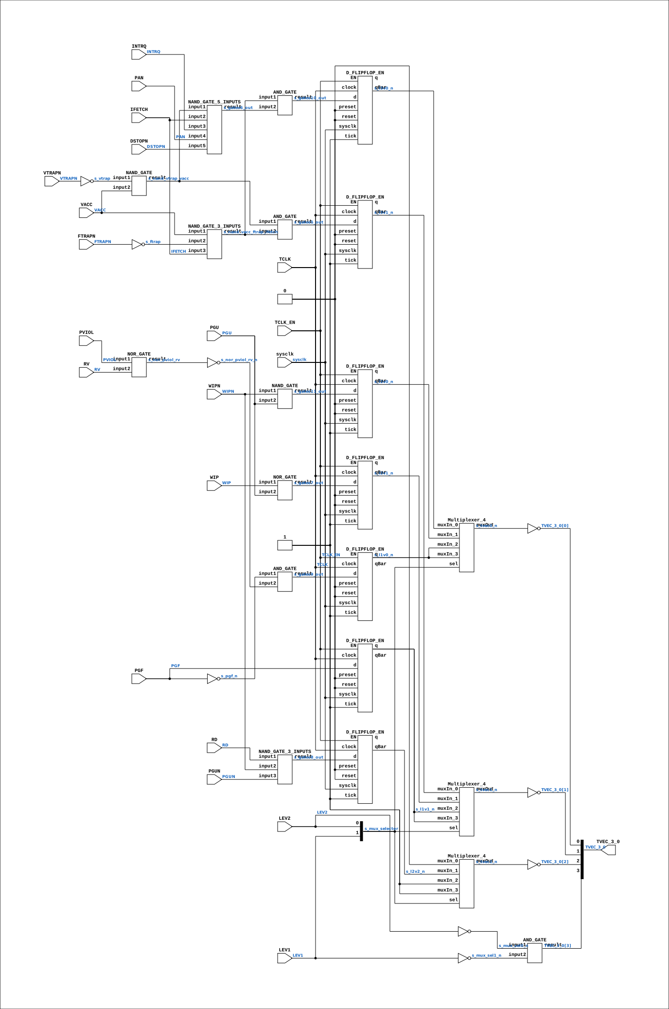
Contains: AND_GATE x4, D_FLIPFLOP_EN x7, Multiplexer_4 x3, NAND_GATE x2, NAND_GATE_3_INPUTS x2, NAND_GATE_5_INPUTS, NOR_GATE x2
Module hierarchy - All modules
Schematic
Drawn from the Verilog: the yosys netlist of the Simulation (Verilator) build, instance CORE.CPU_BOARD.CPU.PROC.CGA.DELILAH.TRAP.TVGEN.TRAP_TVGEN. Sub-modules are boxes (click the picture to open it full size; there every sub-module box links to its page, and every wire shows its Verilog name).
Description
ND120 CGA (CPU Gate Array / DELILAH) /CGA/TRAP/TVGEN/P2 P2 Page 104 SHEET 2 of 2 Last reviewed: 19-JAN-2025 Ronny Hansen
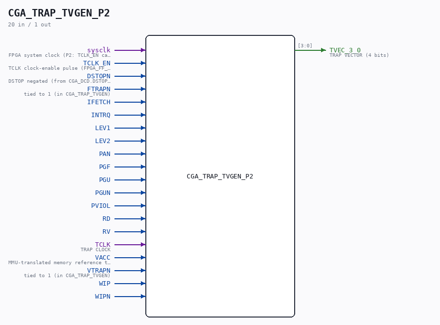
Ports
| Direction | Width | Name | Description |
|---|---|---|---|
| input | 1 |
sysclk |
FPGA system clock (P2: TCLK_EN capture) |
| input | 1 |
TCLK_EN |
TCLK clock-enable pulse (FPGA_FF_MODE, else 0) |
| input | 1 |
DSTOPN |
DSTOP negated (from CGA_DCD.DSTOPN) |
| input | 1 |
FTRAPN |
tied to 1 (in CGA_TRAP_TVGEN) |
| input | 1 |
IFETCH |
|
| input | 1 |
INTRQ |
|
| input | 1 |
LEV1 |
|
| input | 1 |
LEV2 |
|
| input | 1 |
PAN |
|
| input | 1 |
PGF |
|
| input | 1 |
PGU |
|
| input | 1 |
PGUN |
|
| input | 1 |
PVIOL |
|
| input | 1 |
RD |
|
| input | 1 |
RV |
|
| input | 1 |
TCLK |
TRAP CLOCK |
| input | 1 |
VACC |
MMU-translated memory reference this cycle - qualifies the level-2 vector terms |
| input | 1 |
VTRAPN |
tied to 1 (in CGA_TRAP_TVGEN) |
| input | 1 |
WIP |
|
| input | 1 |
WIPN |
|
| output | [3:0] |
TVEC_3_0 |
TRAP VECTOR (4 bits) |
Verilog source
Verilog/DELILAH-CPU/CGA_TRAP/circuit/CGA_TRAP_TVGEN_P2.v on GitHub.
Show the Verilog of CGA_TRAP_TVGEN_P2 (420 lines)
/**************************************************************************
** ND120 CGA (CPU Gate Array / DELILAH)                                  **
** /CGA/TRAP/TVGEN/P2                                                    **
** P2                                                                    **
**                                                                       **
** Page 104                                                              **
** SHEET 2 of 2                                                          **
**                                                                       **
** Last reviewed: 19-JAN-2025                                             **
** Ronny Hansen                                                          **
***************************************************************************/

module CGA_TRAP_TVGEN_P2 (
    input sysclk,   //! FPGA system clock (P2: TCLK_EN capture)
    input TCLK_EN,  //! TCLK clock-enable pulse (FPGA_FF_MODE, else 0)

    input DSTOPN,   //! DSTOP negated (from CGA_DCD.DSTOPN)
    input FTRAPN,   //! tied to 1 (in CGA_TRAP_TVGEN)
    input IFETCH,
    input INTRQ,
    input LEV1,
    input LEV2,
    input PAN,
    input PGF,
    input PGU,
    input PGUN,
    input PVIOL,
    input RD,
    input RV,
    input TCLK,  //! TRAP CLOCK
    input VACC,  //! MMU-translated memory reference this cycle - qualifies the level-2 vector terms
    input VTRAPN,   //! tied to 1 (in CGA_TRAP_TVGEN)
    input WIP,
    input WIPN,


    output [3:0] TVEC_3_0 //! TRAP VECTOR (4 bits)
);

  /*******************************************************************************
   ** The wires are defined here                                                 **
   *******************************************************************************/
  wire [1:0] s_mux_selector;
  wire [3:0] s_tvec_3_0_out;
  wire       s_dstop_n;
  wire       s_ftrap_n;
  wire       s_ftrap;
  wire       s_gates10_out;
  wire       s_gates11_out;
  wire       s_gates5_out;
  wire       s_gates6_out;
  wire       s_gates7_out;
  wire       s_gates8_out;
  wire       s_gates9_out;
  wire       s_gnd;
  wire       s_ifetch;
  wire       s_intrq;
  wire       s_l1v0_n;
  wire       s_l1v1_n;
  wire       s_l2v0_n;
  wire       s_l2v1_n;
  wire       s_l2v2_n;
  wire       s_l3v0_n;
  wire       s_l3v1_n;
  wire       s_mux_sel0_n;
  wire       s_mux_sel1_n;
  wire       s_nand_vacc_ftrap_ifetch;
  wire       s_nand_vtrap_vacc;
  wire       s_nor_pviol_rv_n;
  wire       s_nor_pviol_rv;
  wire       s_pan;
  wire       s_pgf_n;
  wire       s_pgf;
  wire       s_pgu_n;
  wire       s_pgu;
  wire       s_power;
  wire       s_pviol;
  wire       s_rd;
  wire       s_rv;
  wire       s_tclk;
  wire       s_tvec0_n;
  wire       s_tvec1_n;
  wire       s_tvec2_n;
  wire       s_vacc;
  wire       s_vtrap_n;
  wire       s_vtrap;
  wire       s_wip_n;
  wire       s_wip;

  /*******************************************************************************
   ** Here all input connections are defined                                     **
   *******************************************************************************/
  assign s_mux_selector[0] = LEV2;
  assign s_mux_selector[1] = LEV1;
  assign s_dstop_n         = DSTOPN;
  assign s_ftrap_n         = FTRAPN;
  assign s_ifetch          = IFETCH;
  assign s_intrq           = INTRQ;
  assign s_pan             = PAN;
  assign s_pgf             = PGF;
  assign s_pgu             = PGU;
  assign s_pgu_n           = PGUN;
  assign s_pviol           = PVIOL;
  assign s_rd              = RD;
  assign s_rv              = RV;
  assign s_tclk            = TCLK;
  assign s_vacc            = VACC;
  assign s_vtrap_n         = VTRAPN;
  assign s_wip             = WIP;
  assign s_wip_n           = WIPN;

  // P2 (docs/plan-fix-unconstrained-clocks.md): in FF mode the TCLK-
  // clocked registers capture on posedge sysclk gated by TCLK_EN
  // (aligned to the TCLK rise) instead of clocking on the routed net.
`ifdef FPGA_FF_MODE
  localparam TCLK_CE = 1;
`else
  localparam TCLK_CE = 0;
`endif

  /*******************************************************************************
   ** Here all output connections are defined                                    **
   *******************************************************************************/
  assign TVEC_3_0          = s_tvec_3_0_out[3:0];

  /*******************************************************************************
   ** Here all in-lined components are defined                                   **
   *******************************************************************************/

  // Power
  assign s_power           = 1'b1;

  // Ground
  assign s_gnd             = 1'b0;


  // NOT Gate
  assign s_ftrap           = ~s_ftrap_n;
  assign s_nor_pviol_rv_n    = ~s_nor_pviol_rv;
  assign s_mux_sel0_n      = ~s_mux_selector[0];
  assign s_mux_sel1_n      = ~s_mux_selector[1];
  assign s_pgf_n           = ~s_pgf;
  assign s_tvec_3_0_out[2] = ~s_tvec2_n;
  assign s_tvec_3_0_out[1] = ~s_tvec1_n;
  assign s_tvec_3_0_out[0] = ~s_tvec0_n;
  assign s_vtrap           = ~s_vtrap_n;

  /*******************************************************************************
   ** Here all normal components are defined                                     **
   *******************************************************************************/
  AND_GATE #(
      .BubblesMask(2'b00)
  ) GATES_1 (
      .input1(s_mux_sel0_n),
      .input2(s_mux_sel1_n),
      .result(s_tvec_3_0_out[3])
  );

  NAND_GATE_3_INPUTS #(
      .BubblesMask(3'b000)
  ) GATES_2 (
      .input1(s_vacc),
      .input2(s_ftrap),
      .input3(s_ifetch),
      .result(s_nand_vacc_ftrap_ifetch)
  );

  NAND_GATE #(
      .BubblesMask(2'b00)
  ) GATES_3 (
      .input1(s_vtrap),
      .input2(s_vacc),
      .result(s_nand_vtrap_vacc)
  );

  NOR_GATE #(
      .BubblesMask(2'b00)
  ) GATES_4 (
      .input1(s_pviol),
      .input2(s_rv),
      .result(s_nor_pviol_rv)
  );

  AND_GATE #(
      .BubblesMask(2'b00)
  ) GATES_5 (
      .input1(s_nand_vtrap_vacc),
      .input2(s_nand_vacc_ftrap_ifetch),
      .result(s_gates5_out)
  );

  NAND_GATE_5_INPUTS #(
      .BubblesMask({1'b0, 4'h0})
  ) GATES_6 (
      .input1(s_nand_vtrap_vacc),
      .input2(s_ifetch),
      .input3(s_intrq),
      .input4(s_pan),
      .input5(s_dstop_n),
      .result(s_gates6_out)
  );

  NOR_GATE #(
      .BubblesMask(2'b00)
  ) GATES_7 (
      .input1(s_wip),
      .input2(s_pgu),
      .result(s_gates7_out)
  );

  NAND_GATE_3_INPUTS #(
      .BubblesMask(3'b000)
  ) GATES_8 (
      .input1(s_rd),
      .input2(s_wip_n),
      .input3(s_pgu_n),
      .result(s_gates8_out)
  );

  AND_GATE #(
      .BubblesMask(2'b00)
  ) GATES_9 (
      .input1(s_pgf_n),
      .input2(s_nor_pviol_rv_n),
      .result(s_gates9_out)
  );

  AND_GATE #(
      .BubblesMask(2'b00)
  ) GATES_10 (
      .input1(s_nand_vacc_ftrap_ifetch),
      .input2(s_gates6_out),
      .result(s_gates10_out)
  );

  NAND_GATE #(
      .BubblesMask(2'b00)
  ) GATES_11 (
      .input1(s_wip_n),
      .input2(s_pgu),
      .result(s_gates11_out)
  );


  // TVEC 2
  // NOTE (fix 27-JUL): the original schematic (DELILAH p.104) uses a 3-input mux MUX31LP
  // (D0,D1,D2) with A=LEV1 (priority) / B=LEV2 select and an inverting Z output. There is no
  // D3: select A=B=1 maps to D2 (level-1 wins - a page fault must beat a level-2 trap). The
  // Logisim/Verilog conversion modeled it as a 4-input Multiplexer_4 and tied the phantom
  // muxIn_3 to 1'b0, so sel=11 produced TVEC=0111=7 (an unimplemented "SINTRAN 4" trap vector
  // that self-jumps -> hang) whenever a page fault (LEV1) and PGU (LEV2) fired together (e.g.
  // the CX-instruction test's access to a not-present page, IPT=2). Restore the MUX31LP
  // behaviour: muxIn_3 = muxIn_2 (D2) so A=B=1 -> the level-1 (page-fault, vector 1) encoding.
  Multiplexer_4 TVEC2_MUX (
      .muxIn_0(s_gnd),
      .muxIn_1(s_l2v2_n),
      .muxIn_2(s_power),
      .muxIn_3(s_power),   // MUX31LP: A=B=1 selects D2 (=muxIn_2), not a phantom D3
      .muxOut(s_tvec2_n),
      .sel(s_mux_selector[1:0])
  );

  // TVEC 1
  Multiplexer_4 TVEC1_MUX (
      .muxIn_0(s_l3v1_n),
      .muxIn_1(s_l2v1_n),
      .muxIn_2(s_l1v1_n),
      .muxIn_3(s_l1v1_n),  // MUX31LP: A=B=1 selects D2 (=muxIn_2); see TVEC2_MUX note
      .muxOut(s_tvec1_n),
      .sel(s_mux_selector[1:0])
  );

  //TVEC 0
  Multiplexer_4 TVEC0_MUX (
      .muxIn_0(s_l3v0_n),
      .muxIn_1(s_l2v0_n),
      .muxIn_2(s_l1v0_n),
      .muxIn_3(s_l1v0_n),  // MUX31LP: A=B=1 selects D2 (=muxIn_2); see TVEC2_MUX note
      .muxOut(s_tvec0_n),
      .sel(s_mux_selector[1:0])
  );

  // InvertClockEnable(0): fires on the rising edge of s_tclk = posedge TCLK
  D_FLIPFLOP_EN #(
      .USE_ENABLE(TCLK_CE)
  ) L1V0_FF (
      .sysclk(sysclk),
      .EN(TCLK_EN),
      .clock(s_tclk),
      .d(s_gates9_out),
      .preset(1'b0),
      .q(s_l1v0_n),
      .qBar(),
      .reset(1'b0),
      .tick(1'b1)
  );

  // RESTORED 17-AUG-2026 to match the drawing. Page 104 (/CGA/TRAP/TVGEN sheet
  // 2 of 2) draws ALL SEVEN vector bits - L2V2N, L3V1N, L2V1N, L1V1N, L3V0N,
  // L2V0N, L1V0N - as FD1 flip-flops with their CK pins fed from the single
  // TCLK net entering top-left. The level-2 bits are NOT combinational on the
  // sheet.
  //
  // The 27-JUL change replaced these three with `assign s_l2vN_n = ~gate` to
  // cure a trap-vector-7 dispatch (Issue D). That removed a divergence symptom
  // by introducing a divergence: it made the level-2 slot behave differently
  // from the level-1 and level-3 slots, which the drawing treats identically.
  // Since all seven are drawn the same, a stale-capture effect is what the REAL
  // hardware does too, so the real fault must be WHEN TCLK fires relative to
  // the condition becoming valid - not the flip-flops. Chasing that is the
  // point of restoring these.
  //
  // InvertClockEnable(0): fires on the rising edge of s_tclk = posedge TCLK
  D_FLIPFLOP_EN #(
      .USE_ENABLE(TCLK_CE)
  ) L2V2_FF (
      .sysclk(sysclk),
      .EN(TCLK_EN),
      .clock(s_tclk),
      .d(s_gates8_out),
      .preset(1'b0),
      .q(),
      .qBar(s_l2v2_n),
      .reset(1'b0),
      .tick(1'b1)
  );

  // InvertClockEnable(0): fires on the rising edge of s_tclk = posedge TCLK
  D_FLIPFLOP_EN #(
      .USE_ENABLE(TCLK_CE)
  ) L3V1_FF (
      .sysclk(sysclk),
      .EN(TCLK_EN),
      .clock(s_tclk),
      .d(s_gates5_out),
      .preset(1'b0),
      .q(),
      .qBar(s_l3v1_n),
      .reset(1'b0),
      .tick(1'b1)
  );

  // RESTORED 17-AUG-2026 to match page 104 - see the L2V2_FF note above.
  // InvertClockEnable(0): fires on the rising edge of s_tclk = posedge TCLK
  D_FLIPFLOP_EN #(
      .USE_ENABLE(TCLK_CE)
  ) L2V1_FF (
      .sysclk(sysclk),
      .EN(TCLK_EN),
      .clock(s_tclk),
      .d(s_gates7_out),
      .preset(1'b0),
      .q(),
      .qBar(s_l2v1_n),
      .reset(1'b0),
      .tick(1'b1)
  );

  // InvertClockEnable(0): fires on the rising edge of s_tclk = posedge TCLK
  D_FLIPFLOP_EN #(
      .USE_ENABLE(TCLK_CE)
  ) L1V1_FF (
      .sysclk(sysclk),
      .EN(TCLK_EN),
      .clock(s_tclk),
      .d(s_pgf),
      .preset(1'b0),
      .q(s_l1v1_n),
      .qBar(),
      .reset(1'b0),
      .tick(1'b1)
  );

  // InvertClockEnable(0): fires on the rising edge of s_tclk = posedge TCLK
  D_FLIPFLOP_EN #(
      .USE_ENABLE(TCLK_CE)
  ) L3V0_FF (
      .sysclk(sysclk),
      .EN(TCLK_EN),
      .clock(s_tclk),
      .d(s_gates10_out),
      .preset(1'b0),
      .q(),
      .qBar(s_l3v0_n),
      .reset(1'b0),
      .tick(1'b1)
  );

  // RESTORED 17-AUG-2026 to match page 104 - see the L2V2_FF note above.
  // InvertClockEnable(0): fires on the rising edge of s_tclk = posedge TCLK
  D_FLIPFLOP_EN #(
      .USE_ENABLE(TCLK_CE)
  ) L2V0_FF (
      .sysclk(sysclk),
      .EN(TCLK_EN),
      .clock(s_tclk),
      .d(s_gates11_out),
      .preset(1'b0),
      .q(),
      .qBar(s_l2v0_n),
      .reset(1'b0),
      .tick(1'b1)
  );

`ifdef TRAPDBG
  // Internal vector-7 diagnosis: on the cycle the vector first becomes 7, dump
  // the select + every level-condition + the registered l*v* bits, so we can see
  // WHICH sel/condition path produces 7 (algebra says it should be impossible
  // with the mux fix - this settles which assumption is wrong).
  reg r_v7_d = 1'b0;
  always @(posedge sysclk) begin
    r_v7_d <= (s_tvec_3_0_out == 4'd7);
    if (!r_v7_d && (s_tvec_3_0_out == 4'd7))
      $display("[tv7] sel=%b(L1=%b L2=%b) WIP=%b PGU=%b PGF=%b RD=%b RV=%b PVIOL=%b VACC=%b IFE=%b | l2v2n=%b l2v1n=%b l2v0n=%b l1v1n=%b l1v0n=%b l3v1n=%b l3v0n=%b",
        s_mux_selector, LEV1, LEV2, s_wip, s_pgu, s_pgf, s_rd, s_rv, s_pviol, s_vacc, s_ifetch,
        s_l2v2_n, s_l2v1_n, s_l2v0_n, s_l1v1_n, s_l1v0_n, s_l3v1_n, s_l3v0_n);
  end
`endif

endmodule