CGA_INTR
Source: Verilog/DELILAH-CPU/CGA_INTR/circuit/CGA_INTR.v
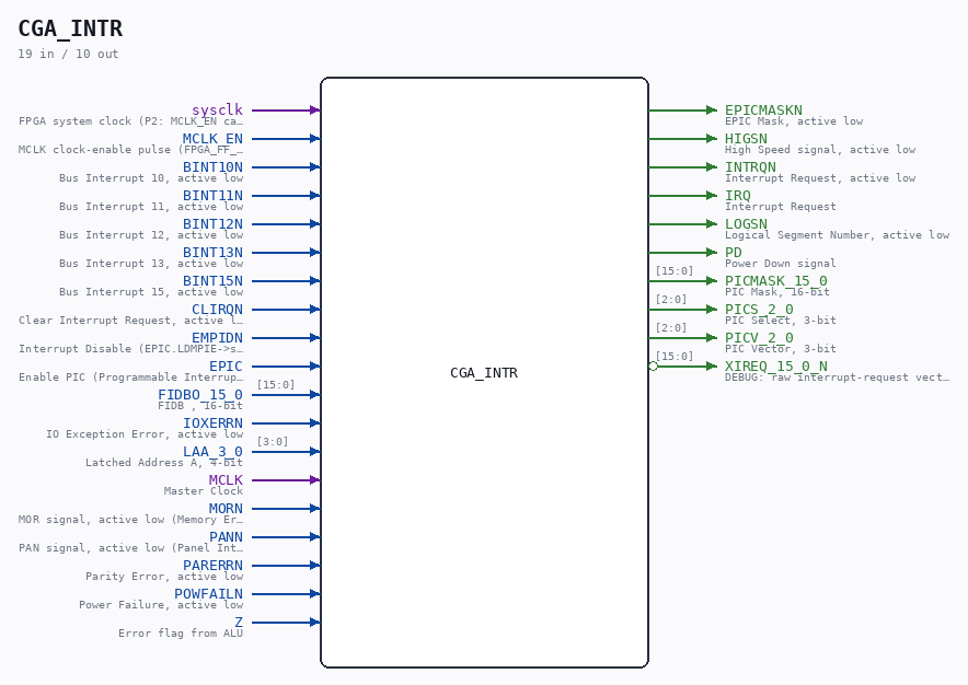
Where it sits (Simulation): ND120_TOP > ND120_CORE > ND3202D > CPU_15 > CPU_PROC_32 > CPU_PROC_CGA_33 > CGA > CGA_INTR
- instance path: CORE.CPU_BOARD.CPU.PROC.CGA.DELILAH.INTR
Used in: CGA (all tops)
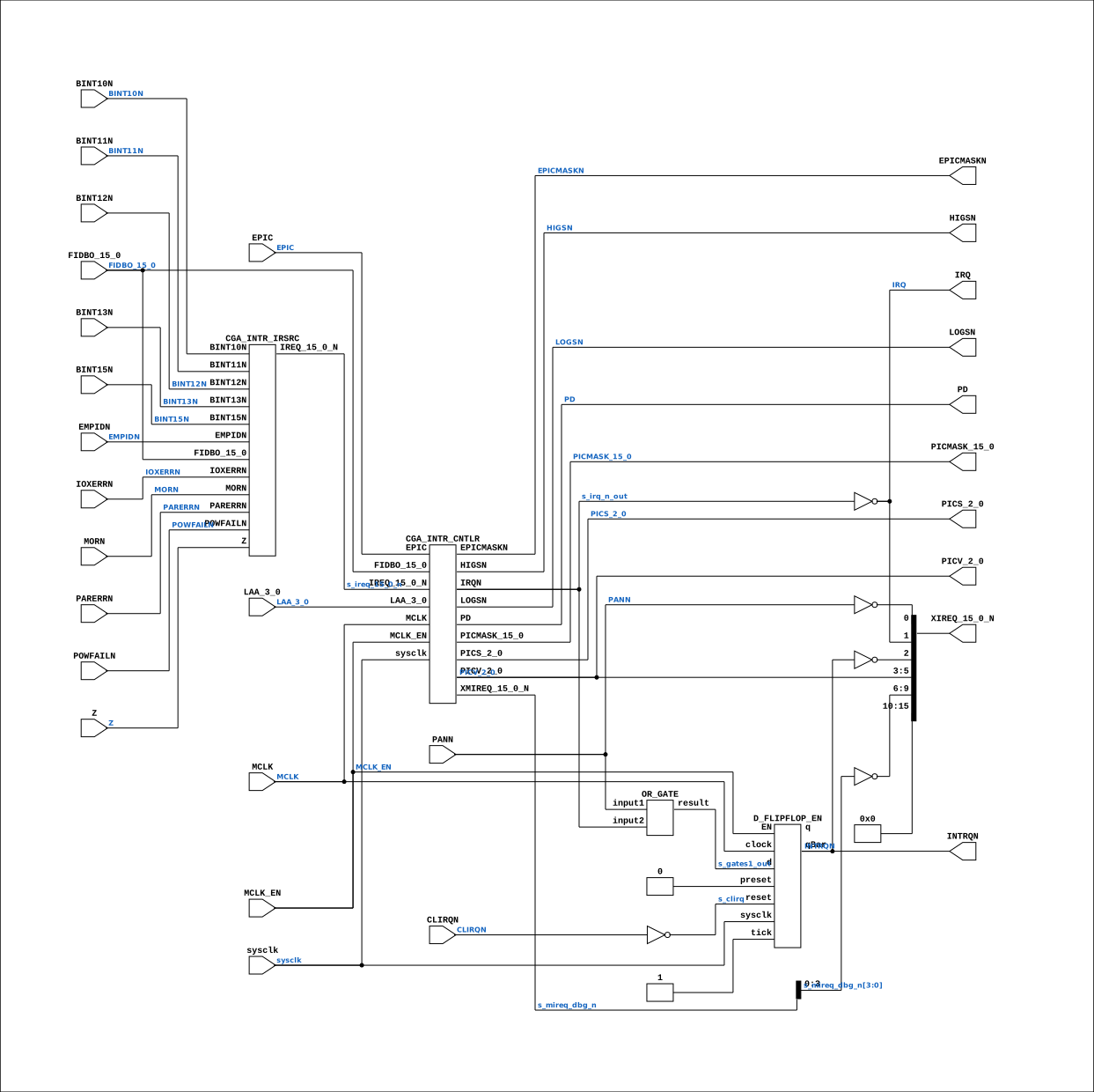
Contains: CGA_INTR_CNTLR, CGA_INTR_IRSRC, D_FLIPFLOP_EN, OR_GATE
Module hierarchy - All modules
Schematic
Drawn from the Verilog: the yosys netlist of the Simulation (Verilator) build, instance CORE.CPU_BOARD.CPU.PROC.CGA.DELILAH.INTR. Sub-modules are boxes (click the picture to open it full size; there every sub-module box links to its page, and every wire shows its Verilog name).
Description
CPU GATE ARRAY - CGA - DELILAH CGA/INTR Sheet 1 of 1 PDF page 74 Last reviewed: 26-JAN-2025 Ronny Hansen
Ports
| Direction | Width | Name | Description |
|---|---|---|---|
| input | 1 |
sysclk |
FPGA system clock (P2: MCLK_EN capture) |
| input | 1 |
MCLK_EN |
MCLK clock-enable pulse (FPGA_FF_MODE, else 0) |
| input | 1 |
BINT10N |
Bus Interrupt 10, active low |
| input | 1 |
BINT11N |
Bus Interrupt 11, active low |
| input | 1 |
BINT12N |
Bus Interrupt 12, active low |
| input | 1 |
BINT13N |
Bus Interrupt 13, active low |
| input | 1 |
BINT15N |
Bus Interrupt 15, active low |
| input | 1 |
CLIRQN |
Clear Interrupt Request, active low |
| input | 1 |
EMPIDN |
Interrupt Disable (EPIC.LDMPIE->set mask reg:inh all ints) |
| input | 1 |
EPIC |
Enable PIC (Programmable Interrupt Controller) signal |
| input | [15:0] |
FIDBO_15_0 |
FIDB , 16-bit |
| input | 1 |
IOXERRN |
IO Exception Error, active low |
| input | [3:0] |
LAA_3_0 |
Latched Address A, 4-bit |
| input | 1 |
MCLK |
Master Clock |
| input | 1 |
MORN |
MOR signal, active low (Memory Error) |
| input | 1 |
PANN |
PAN signal, active low (Panel Interrupt) |
| input | 1 |
PARERRN |
Parity Error, active low |
| input | 1 |
POWFAILN |
Power Failure, active low |
| input | 1 |
Z |
Error flag from ALU |
| output | 1 |
EPICMASKN |
EPIC Mask, active low |
| output | 1 |
HIGSN |
High Speed signal, active low |
| output | 1 |
INTRQN |
Interrupt Request, active low |
| output | 1 |
IRQ |
Interrupt Request |
| output | 1 |
LOGSN |
Logical Segment Number, active low |
| output | 1 |
PD |
Power Down signal |
| output | [15:0] |
PICMASK_15_0 |
PIC Mask, 16-bit |
| output | [2:0] |
PICS_2_0 |
PIC Select, 3-bit |
| output | [2:0] |
PICV_2_0 |
PIC Vector, 3-bit |
| output | [15:0] |
XIREQ_15_0_N (active low) |
DEBUG: raw interrupt-request vector (active low) for grant-source capture |
Verilog source
Verilog/DELILAH-CPU/CGA_INTR/circuit/CGA_INTR.v on GitHub.
Show the Verilog of CGA_INTR (256 lines)
/**************************************************************************
** CPU GATE ARRAY - CGA - DELILAH                                        **
**                                                                       **
** CGA/INTR                                                              **
**                                                                       **
** Sheet 1 of 1                                                          **
** PDF page 74                                                           **
**                                                                       **
** Last reviewed: 26-JAN-2025                                            **
** Ronny Hansen                                                          **
***************************************************************************/

module CGA_INTR (
    input        sysclk,           //! FPGA system clock (P2: MCLK_EN capture)
    input        MCLK_EN,          //! MCLK clock-enable pulse (FPGA_FF_MODE, else 0)

    input        BINT10N,          //! Bus Interrupt 10, active low
    input        BINT11N,          //! Bus Interrupt 11, active low
    input        BINT12N,          //! Bus Interrupt 12, active low
    input        BINT13N,          //! Bus Interrupt 13, active low
    input        BINT15N,          //! Bus Interrupt 15, active low
    input        CLIRQN,           //! Clear Interrupt Request, active low
    input        EMPIDN,           //! Interrupt Disable (EPIC.LDMPIE->set mask reg:inh all ints)
    input        EPIC,             //! Enable PIC (Programmable Interrupt Controller) signal
    input [15:0] FIDBO_15_0,       //! FIDB , 16-bit
    input        IOXERRN,          //! IO Exception Error, active low
    input [ 3:0] LAA_3_0,          //! Latched Address A, 4-bit
    input        MCLK,             //! Master Clock
    input        MORN,             //! MOR signal, active low (Memory Error)
    input        PANN,             //! PAN signal, active low (Panel Interrupt)
    input        PARERRN,          //! Parity Error, active low
    input        POWFAILN,         //! Power Failure, active low
    input        Z,                //! Error flag from ALU

    output        EPICMASKN,       //! EPIC Mask, active low
    output        HIGSN,           //! High Speed signal, active low
    output        INTRQN,          //! Interrupt Request, active low
    output        IRQ,             //! Interrupt Request
    output        LOGSN,           //! Logical Segment Number, active low
    output        PD,              //! Power Down signal
    output [15:0] PICMASK_15_0,    //! PIC Mask, 16-bit
    output [ 2:0] PICS_2_0,        //! PIC Select, 3-bit
    output [ 2:0] PICV_2_0,        //! PIC Vector, 3-bit
    output [15:0] XIREQ_15_0_N     //! DEBUG: raw interrupt-request vector (active low) for grant-source capture
);

  /*******************************************************************************
   ** The wires are defined here                                                 **
   *******************************************************************************/
  wire [15:0] s_fidbo_15_0;
  wire [15:0] s_picmask_15_0_out;
  wire [ 2:0] s_picv_2_0_out /* synthesis syn_keep=1 */;  // GAO probe net - see fpga/tang-nano-20k/GAO-HOWTO.md
  wire [ 2:0] s_pics_2_0_out;
  wire [ 3:0] s_laa_3_0;
  wire [15:0] s_ireq_15_0_n /* synthesis syn_keep=1 */;  // GAO probe net
  wire        s_bint10_n;
  wire        s_bint11_n;
  wire        s_bint12_n;
  wire        s_bint13_n;
  wire        s_bint15_n;
  wire        s_clirq_n;
  wire        s_clirq;
  wire        s_empid_n;
  wire        s_epic;
  wire        s_epicmask_n_out;
  wire        s_gates1_out;
  wire        s_highs_n_out;
  wire        s_intrq_n /* synthesis syn_keep=1 */;  // GAO probe net
  wire        s_ioxerr_n;
  wire        s_irq_n_out;
  wire        s_irq_out;
  wire        s_logs_n_out;
  wire        s_mclk /* synthesis syn_keep=1 */;  // GAO probe net
  wire        s_mor_n;
  wire        s_pan_n;
  wire        s_parerr_n;
  wire        s_pd_out;
  wire        s_powfail_n;
  wire        s_z;

  /*******************************************************************************
   ** The module functionality is described here                                 **
   *******************************************************************************/

   reg [3:0] regLAA_3_0;

  /*******************************************************************************
   ** Here all input connections are defined                                     **
   *******************************************************************************/
  assign s_bint10_n         = BINT10N;
  assign s_bint11_n         = BINT11N;
  assign s_bint12_n         = BINT12N;
  assign s_bint13_n         = BINT13N;
  assign s_bint15_n         = BINT15N;
  assign s_clirq_n          = CLIRQN;
  assign s_empid_n          = EMPIDN;
  assign s_epic             = EPIC;
  assign s_fidbo_15_0[15:0] = FIDBO_15_0;
`ifdef TANG_NO_IOXERR
  // DIAGNOSTIC (masked-level-10 root cause): drop the IOX/bus-timeout error
  // request (IREQ bit 10 = level 10, NOT enable-gated). If the phantom level-10
  // wedge vanishes, a spurious bus timeout (TOUT) on the Tang is the source.
  assign s_ioxerr_n         = 1'b1;
`else
  assign s_ioxerr_n         = IOXERRN;
`endif

  //assign s_laa_3_0[3:0]     = LAA_3_0;
  assign s_laa_3_0[3:0]     = regLAA_3_0;

  assign s_mclk             = MCLK;

  // P2 (docs/plan-fix-unconstrained-clocks.md): in FF mode the MCLK-
  // clocked registers capture on posedge sysclk gated by MCLK_EN
  // (aligned to the MCLK rise) instead of clocking on the routed net.
`ifdef FPGA_FF_MODE
  localparam MCLK_CE = 1;
`else
  localparam MCLK_CE = 0;
`endif

`ifdef ND120_MOR_TIED_OFF
  assign s_mor_n            = 1'b1;   // B2 experiment: MOR source disabled (diagnostic only)
`else
  assign s_mor_n            = MORN;  // Memory Out of Range (active low), from board MOR_n via CGA.XMORN
`endif
`ifdef TANG_NO_PAN
  // DIAGNOSTIC: hard-disable the panel (PAN) input to INTRQN entirely. If the
  // phantom level-10 grant vanishes, PAN (some panel/PRQ source) was the
  // trigger; if it persists, INTRQN is set by an IRQ-path glitch (MIREQ was
  // measured empty, so a genuine masked request is NOT the cause).
  assign s_pan_n            = 1'b1;
`else
  assign s_pan_n            = PANN;
`endif
  assign s_parerr_n         = PARERRN;
  assign s_powfail_n        = POWFAILN;
  assign s_z                = Z;

  /*******************************************************************************
   ** Here all output connections are defined                                    **
   *******************************************************************************/
  assign EPICMASKN          = s_epicmask_n_out;
  assign HIGSN              = s_highs_n_out;
  assign INTRQN             = s_intrq_n;
  assign IRQ                = s_irq_out;

`ifdef ND120_ILA_MARK_DEBUG
  // 25-AUG SINTRAN-idle hunt (Nexys): the machine idles at PIL 0 and no
  // interrupt ever dispatches. Capture the controller's own view: the PIC
  // mask (PIE as the Am2914 chain sees it), the grant request to the
  // microcode, and the winning vector.
  (* mark_debug = "true" *) wire [15:0] s_ila_picmask = s_picmask_15_0_out;
  (* mark_debug = "true" *) wire        s_ila_intrq_n = s_intrq_n;
  (* mark_debug = "true" *) wire [ 2:0] s_ila_picv    = s_picv_2_0_out[2:0];
`endif
  assign LOGSN              = s_logs_n_out;
  assign PD                 = s_pd_out;
  assign PICMASK_15_0       = s_picmask_15_0_out[15:0];
  assign PICS_2_0           = s_pics_2_0_out[2:0];
  assign PICV_2_0           = s_picv_2_0_out[2:0];
  // DEBUG capture word (active-HIGH; the Tang top captures it directly, no invert):
  //   bit0=PAN  bit1=IRQ  bit2=INTRQ  bit5:3=PICV[2:0]  bit9:6=MIREQ low nibble
  // This shows, at the dispatch, whether PAN pulses (INTRQN from panel, not a
  // request) and that PICV reads empty (0) -> the stale-INTRQN -> macro -> level 10.
  wire [15:0] s_mireq_dbg_n;
  assign XIREQ_15_0_N       = { 6'b0,
                                (~s_mireq_dbg_n[3:0]),   // bit9:6 = MIREQ[3:0] active-high
                                s_picv_2_0_out[2:0],     // bit5:3 = PICV
                                (~s_intrq_n),            // bit2   = INTRQ (grant asserted)
                                s_irq_out,               // bit1   = IRQ (Am2914 claim)
                                (~s_pan_n) };            // bit0   = PAN (panel request)

  /*******************************************************************************
   ** Here all in-lined components are defined                                   **
   *******************************************************************************/

  // Need to add delay to changing of LAA_3_0 so that if it changes when MCLK changes we dont get the "new and wrong value"
  // TODO: Review if this can be solved with rising edge on sysclk
  always @(LAA_3_0)
  begin
    regLAA_3_0 <= LAA_3_0;
  end

  // NOT Gate
  assign s_irq_out          = ~s_irq_n_out;
  assign s_clirq            = ~s_clirq_n;

  /*******************************************************************************
   ** Here all normal components are defined                                     **
   *******************************************************************************/
  OR_GATE #(
      .BubblesMask(2'b11)
  ) GATES_1 (
      .input1(s_pan_n),
      .input2(s_irq_n_out),
      .result(s_gates1_out)
  );

  // MCLK domain (CGA_INTR.MCLK, rising edge); async clear via CLIRQN
  D_FLIPFLOP_EN #(
      .USE_ENABLE(MCLK_CE),
      .ASYNC_RESET(1)
  ) MEMORY_2 (
      .sysclk(sysclk),
      .EN(MCLK_EN),
      .clock(s_mclk),
      .d(s_gates1_out),
      .preset(1'b0),
      .q(),
      .qBar(s_intrq_n),
      .reset(s_clirq),
      .tick(1'b1)
  );


  /*******************************************************************************
   ** Here all sub-circuits are defined                                          **
   *******************************************************************************/

  CGA_INTR_CNTLR CNTLR (
      .sysclk(sysclk),
      .MCLK_EN(MCLK_EN),
      .EPIC(s_epic),
      .EPICMASKN(s_epicmask_n_out),
      .FIDBO_15_0(s_fidbo_15_0[15:0]),
      .HIGSN(s_highs_n_out),
      .IREQ_15_0_N(s_ireq_15_0_n[15:0]),
      .IRQN(s_irq_n_out),
      .LAA_3_0(s_laa_3_0[3:0]),
      .LOGSN(s_logs_n_out),
      .MCLK(s_mclk),
      .PD(s_pd_out),
      .PICMASK_15_0(s_picmask_15_0_out[15:0]),
      .PICS_2_0(s_pics_2_0_out[2:0]),
      .PICV_2_0(s_picv_2_0_out[2:0]),
      .XMIREQ_15_0_N(s_mireq_dbg_n)
  );

  CGA_INTR_IRSRC IRSRC (
      .BINT10N(s_bint10_n),
      .BINT11N(s_bint11_n),
      .BINT12N(s_bint12_n),
      .BINT13N(s_bint13_n),
      .BINT15N(s_bint15_n),
      .EMPIDN(s_empid_n),
      .FIDBO_15_0(s_fidbo_15_0[15:0]),
      .IOXERRN(s_ioxerr_n),
      .IREQ_15_0_N(s_ireq_15_0_n[15:0]),
      .MORN(s_mor_n),
      .PARERRN(s_parerr_n),
      .POWFAILN(s_powfail_n),
      .Z(s_z)
  );

endmodule