CGA_ALU_SWAP
Source: Verilog/DELILAH-CPU/CGA_ALU/circuit/CGA_ALU_SWAP.v
Where it sits (Simulation): ND120_TOP > ND120_CORE > ND3202D > CPU_15 > CPU_PROC_32 > CPU_PROC_CGA_33 > CGA > CGA_ALU > CGA_ALU_SWAP
- instance path: CORE.CPU_BOARD.CPU.PROC.CGA.DELILAH.ALU.ALU_SWAP
Used in: CGA_ALU (all tops)
Contains: R81_EN x2
Module hierarchy - All modules
Schematic
Drawn from the Verilog: the yosys netlist of the Simulation (Verilator) build, instance CORE.CPU_BOARD.CPU.PROC.CGA.DELILAH.ALU.ALU_SWAP. Sub-modules are boxes (click the picture to open it full size; there every sub-module box links to its page, and every wire shows its Verilog name).
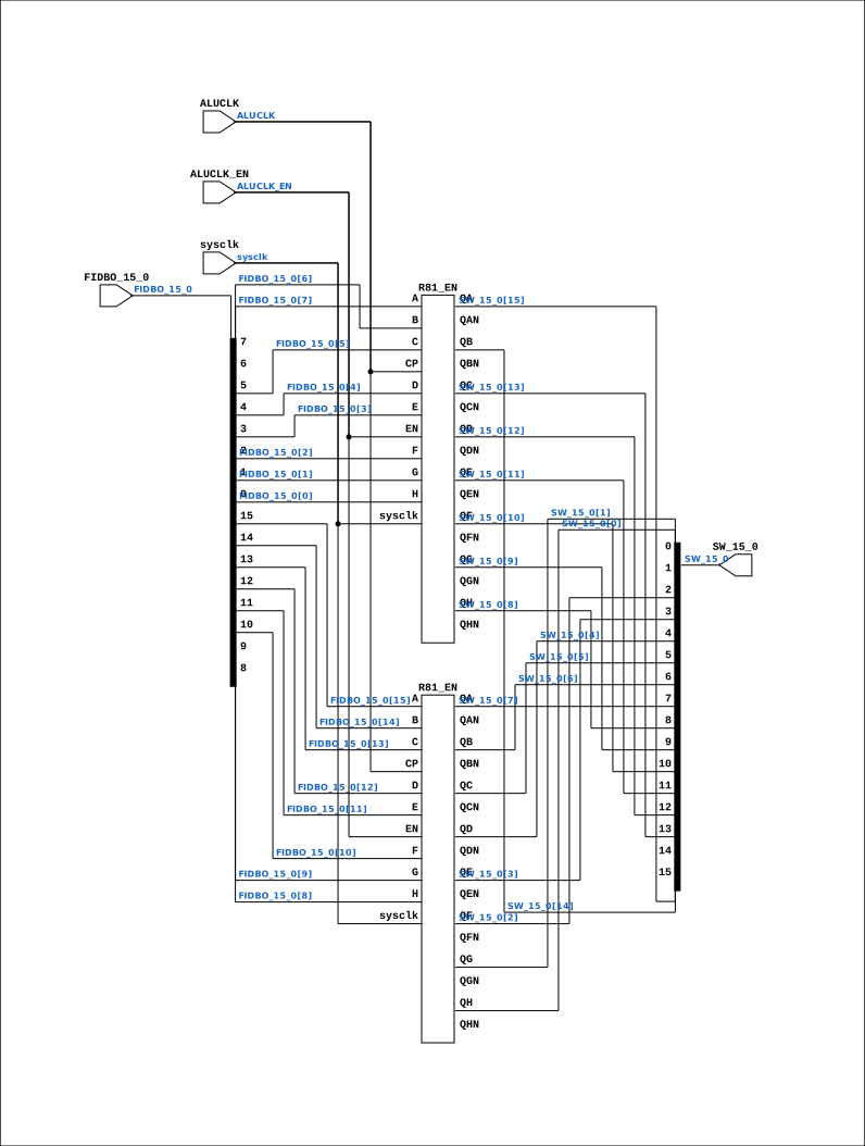
Description
ND120 CGA (CPU Gate Array / DELILAH) /CGA/ALU/SWAP SWAP REGISTER Page 51 SHEET 1 of 1 Last reviewed: 10-NOV-2024 Ronny Hansen
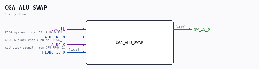
Ports
| Direction | Width | Name | Description |
|---|---|---|---|
| input | 1 |
sysclk |
FPGA system clock (P2: ALUCLK_EN capture) |
| input | 1 |
ALUCLK_EN |
ALUCLK clock-enable pulse (FPGA_FF_MODE, else 0) |
| input | 1 |
ALUCLK |
ALU clock signal (from CPU_PROC_CGA_33.ALUCLK) |
| input | [15:0] |
FIDBO_15_0 |
|
| output | [15:0] |
SW_15_0 |
Verilog source
Verilog/DELILAH-CPU/CGA_ALU/circuit/CGA_ALU_SWAP.v on GitHub.
Show the Verilog of CGA_ALU_SWAP (115 lines)
/**************************************************************************
** ND120 CGA (CPU Gate Array / DELILAH)                                  **
** /CGA/ALU/SWAP                                                         **
** SWAP REGISTER                                                         **
**                                                                       **
** Page 51                                                               **
** SHEET 1 of 1                                                          **
**                                                                       **
** Last reviewed: 10-NOV-2024                                            **
** Ronny Hansen                                                          **
***************************************************************************/


module CGA_ALU_SWAP (
    input        sysclk,     //! FPGA system clock (P2: ALUCLK_EN capture)
    input        ALUCLK_EN,  //! ALUCLK clock-enable pulse (FPGA_FF_MODE, else 0)
    input        ALUCLK,     //! ALU clock signal (from CPU_PROC_CGA_33.ALUCLK)
    input [15:0] FIDBO_15_0,

    output [15:0] SW_15_0
);

  /*******************************************************************************
   ** The wires are defined here                                                 **
   *******************************************************************************/
  wire [15:0] s_fidbo_15_0;
  wire [15:0] s_sw_15_0_out;
  wire        s_aluclk;

  /*******************************************************************************
   ** Here all input connections are defined                                     **
   *******************************************************************************/
  assign s_fidbo_15_0[15:0] = FIDBO_15_0;
  assign s_aluclk           = ALUCLK;

  // P2b (docs/plan-fix-unconstrained-clocks.md): in FF mode the ALUCLK-
  // clocked registers capture on posedge sysclk gated by ALUCLK_EN
  // (aligned to the ALUCLK rise) instead of clocking on the routed net.
`ifdef FPGA_FF_MODE
  localparam ALUCLK_CE = 1;
`else
  localparam ALUCLK_CE = 0;
`endif


  /*******************************************************************************
   ** Here all output connections are defined                                    **
   *******************************************************************************/
  assign SW_15_0            = s_sw_15_0_out[15:0];

  /*******************************************************************************
   ** Here all sub-circuits are defined                                          **
   *******************************************************************************/

  R81_EN #(.USE_ENABLE(ALUCLK_CE)) SWAP_LO_REG (
      .sysclk(sysclk),
      .EN(ALUCLK_EN),
      .CP(s_aluclk),
      .A  (s_fidbo_15_0[15]),
      .B  (s_fidbo_15_0[14]),
      .C  (s_fidbo_15_0[13]),
      .D  (s_fidbo_15_0[12]),
      .E  (s_fidbo_15_0[11]),
      .F  (s_fidbo_15_0[10]),
      .G  (s_fidbo_15_0[9]),
      .H  (s_fidbo_15_0[8]),
      .QA (s_sw_15_0_out[7]),
      .QAN(),
      .QB (s_sw_15_0_out[6]),
      .QBN(),
      .QC (s_sw_15_0_out[5]),
      .QCN(),
      .QD (s_sw_15_0_out[4]),
      .QDN(),
      .QE (s_sw_15_0_out[3]),
      .QEN(),
      .QF (s_sw_15_0_out[2]),
      .QFN(),
      .QG (s_sw_15_0_out[1]),
      .QGN(),
      .QH (s_sw_15_0_out[0]),
      .QHN()
  );

  R81_EN #(.USE_ENABLE(ALUCLK_CE)) SWAP_HI_REG (
      .sysclk(sysclk),
      .EN(ALUCLK_EN),
      .CP(s_aluclk),
      .A  (s_fidbo_15_0[7]),
      .B  (s_fidbo_15_0[6]),
      .C  (s_fidbo_15_0[5]),
      .D  (s_fidbo_15_0[4]),
      .E  (s_fidbo_15_0[3]),
      .F  (s_fidbo_15_0[2]),
      .G  (s_fidbo_15_0[1]),
      .H  (s_fidbo_15_0[0]),
      .QA (s_sw_15_0_out[15]),
      .QAN(),
      .QB (s_sw_15_0_out[14]),
      .QBN(),
      .QC (s_sw_15_0_out[13]),
      .QCN(),
      .QD (s_sw_15_0_out[12]),
      .QDN(),
      .QE (s_sw_15_0_out[11]),
      .QEN(),
      .QF (s_sw_15_0_out[10]),
      .QFN(),
      .QG (s_sw_15_0_out[9]),
      .QGN(),
      .QH (s_sw_15_0_out[8]),
      .QHN()
  );

endmodule