CGA_MAC_LASEL
Source: Verilog/DELILAH-CPU/CGA_MAC/circuit/CGA_MAC_LASEL.v
Where it sits (Simulation): ND120_TOP > ND120_CORE > ND3202D > CPU_15 > CPU_PROC_32 > CPU_PROC_CGA_33 > CGA > CGA_MAC > CGA_MAC_LASEL
- instance path: CORE.CPU_BOARD.CPU.PROC.CGA.DELILAH.MAC.MAC_LASEL
Used in: CGA_MAC (all tops)
Contains: AND_GATE x8, AND_GATE_3_INPUTS, AND_GATE_4_INPUTS x3, D_FLIPFLOP_EN, NAND_GATE x4, NAND_GATE_3_INPUTS, NAND_GATE_5_INPUTS x2, NOR_GATE, OR_GATE x2, OR_GATE_3_INPUTS
Module hierarchy - All modules
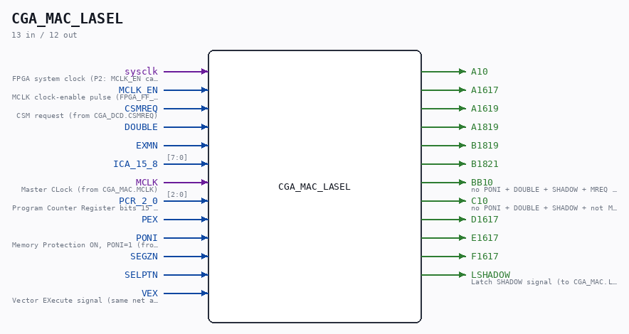
Schematic
Drawn from the Verilog: the yosys netlist of the Simulation (Verilator) build, instance CORE.CPU_BOARD.CPU.PROC.CGA.DELILAH.MAC.MAC_LASEL. Sub-modules are boxes (click the picture to open it full size; there every sub-module box links to its page, and every wire shows its Verilog name).
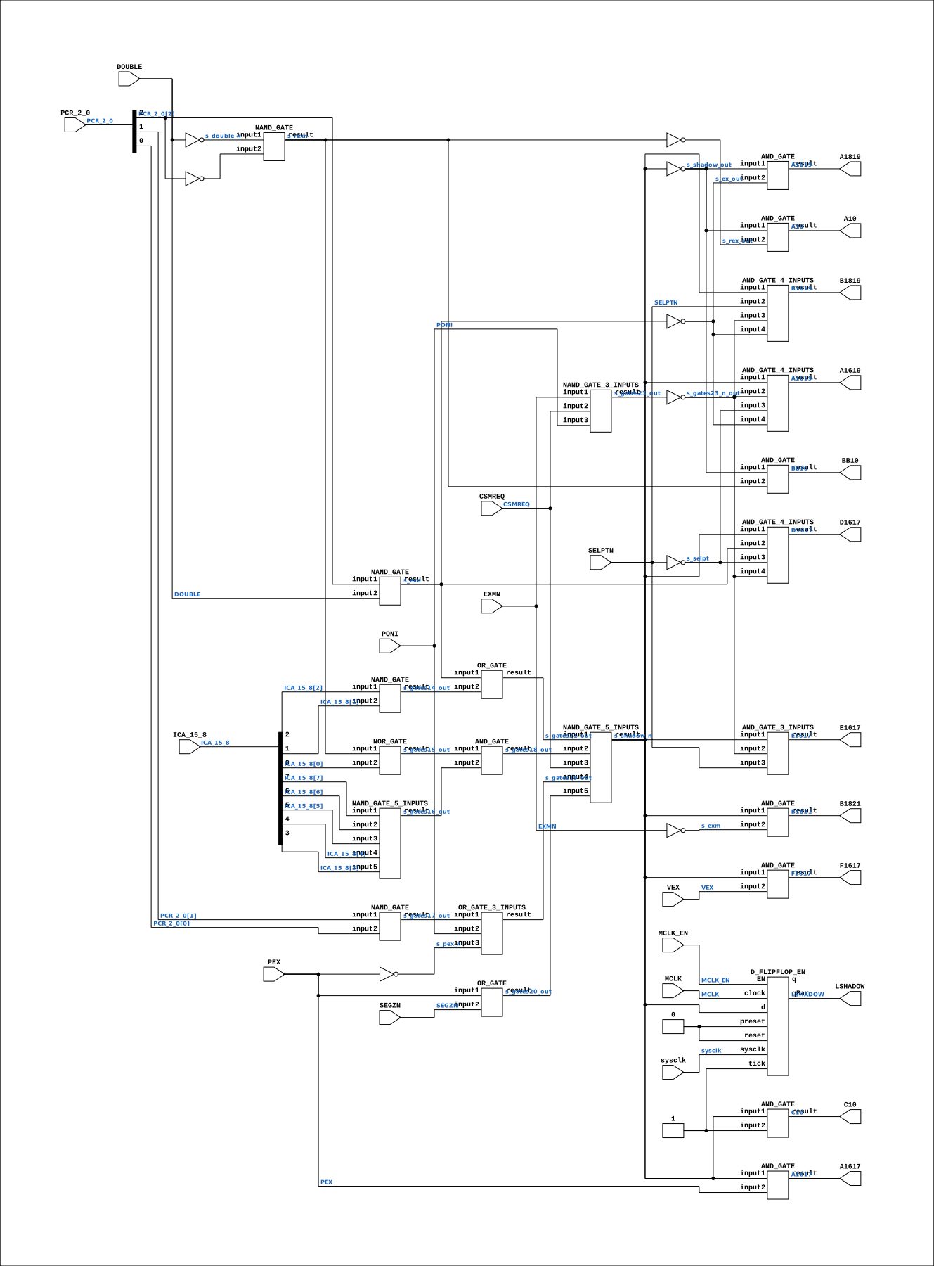
Description
ND120 CGA (CPU Gate Array / DELILAH) /CGA/MAC/LASEL LASEL Page 39 SHEET 1 of 1 Last reviewed: 02-FEB-2025 Ronny Hansen 02-FEB-2025 - Refactored and renamed PCR_15_7_2_0 to PCR_2_0 Refactored ICA_15_8 to use 8 bits, not 16
Ports
| Direction | Width | Name | Description |
|---|---|---|---|
| input | 1 |
sysclk |
FPGA system clock (P2: MCLK_EN capture) |
| input | 1 |
MCLK_EN |
MCLK clock-enable pulse (FPGA_FF_MODE, else 0) |
| input | 1 |
CSMREQ |
CSM request (from CGA_DCD.CSMREQ) |
| input | 1 |
DOUBLE |
|
| input | 1 |
EXMN |
|
| input | [7:0] |
ICA_15_8 |
|
| input | 1 |
MCLK |
Master CLock (from CGA_MAC.MCLK) |
| input | [2:0] |
PCR_2_0 |
Program Counter Register bits 15 to 0 (same net as CGA_MAC.PCR_15_0[2:0]) |
| input | 1 |
PEX |
|
| input | 1 |
PONI |
Memory Protection ON, PONI=1 (from CGA_MAC.PONI) |
| input | 1 |
SEGZN |
|
| input | 1 |
SELPTN |
|
| input | 1 |
VEX |
Vector EXecute signal (same net as CGA_MAC.VEX) |
| output | 1 |
A10 |
|
| output | 1 |
A1617 |
|
| output | 1 |
A1619 |
|
| output | 1 |
A1819 |
|
| output | 1 |
B1819 |
|
| output | 1 |
B1821 |
|
| output | 1 |
BB10 |
no PONI + DOUBLE + SHADOW + MREQ (to CGA_MAC_LA1025.BB10) |
| output | 1 |
C10 |
no PONI + DOUBLE + SHADOW + not MREQ (to CGA_MAC_LA1025.C10) |
| output | 1 |
D1617 |
|
| output | 1 |
E1617 |
|
| output | 1 |
F1617 |
|
| output | 1 |
LSHADOW |
Latch SHADOW signal (to CGA_MAC.LSHADOW) |
Verilog source
Verilog/DELILAH-CPU/CGA_MAC/circuit/CGA_MAC_LASEL.v on GitHub.
Show the Verilog of CGA_MAC_LASEL (432 lines)
/**************************************************************************
** ND120 CGA (CPU Gate Array / DELILAH)                                  **
** /CGA/MAC/LASEL                                                        **
** LASEL                                                                 **
**                                                                       **
** Page 39                                                               **
** SHEET 1 of 1                                                          **
**                                                                       **
** Last reviewed: 02-FEB-2025                                            **
** Ronny Hansen                                                          **
**                                                                       **
** 02-FEB-2025 - Refactored and renamed PCR_15_7_2_0 to PCR_2_0          **
**               Refactored ICA_15_8 to use 8 bits, not 16               **
***************************************************************************/

module CGA_MAC_LASEL (
    input        sysclk,   //! FPGA system clock (P2: MCLK_EN capture)
    input        MCLK_EN,  //! MCLK clock-enable pulse (FPGA_FF_MODE, else 0)

    input        CSMREQ,   //! CSM request (from CGA_DCD.CSMREQ)
    input        DOUBLE,
    input        EXMN,
    input [7:0]  ICA_15_8,
    input        MCLK,     //! Master CLock (from CGA_MAC.MCLK)
    input [2:0]  PCR_2_0,  //! Program Counter Register bits 15 to 0 (same net as CGA_MAC.PCR_15_0[2:0])
    input        PEX,
    input        PONI,     //! Memory Protection ON, PONI=1 (from CGA_MAC.PONI)
    input        SEGZN,
    input        SELPTN,
    input        VEX,      //! Vector EXecute signal (same net as CGA_MAC.VEX)

    output A10,
    output A1617,
    output A1619,
    output A1819,
    output B1819,
    output B1821,
    output BB10,           //! no PONI + DOUBLE + SHADOW + MREQ (to CGA_MAC_LA1025.BB10)
    output C10,            //! no PONI + DOUBLE + SHADOW + not MREQ (to CGA_MAC_LA1025.C10)
    output D1617,
    output E1617,
    output F1617,
    output LSHADOW         //! Latch SHADOW signal (to CGA_MAC.LSHADOW)
);

  /*******************************************************************************
   ** The wires are defined here                                                 **
   *******************************************************************************/
  wire [7:0]  s_ica_15_8;
  wire [2:0]  s_pcr_2_0;
  wire        a_1617_out;
  wire        c_csmreq;
  wire        s_a10_out;
  wire        s_a1619_out;
  wire        s_a1819_out;
  wire        s_b1819_out;
  wire        s_b1821_out;
  wire        s_bb10_out;
  wire        s_c10_out;
  wire        s_d1617_out;
  wire        s_double_n;
  wire        s_double;
  wire        s_e1617_out;
  wire        s_exm_n;
  wire        s_exm;
  wire        s_f1617_out;
  wire        s_rex_out;
  wire        s_rexn;
  wire        s_ex_out;
  wire        s_exn;
  wire        s_gates14_out;
  wire        s_gates15_out;
  wire        s_gates16_out;
  wire        s_gates17_out;
  wire        s_gates18_out;
  wire        s_gates19_out;
  wire        s_gates20_out;
  wire        s_gates21_out;
  wire        s_shadow_out;
  wire        s_shadow_n;
  wire        s_gates23_n_out;
  wire        s_gates23_out;
  wire        s_lshadow;
  wire        s_mclk;
  wire        s_pex_n;
  wire        s_pex;
  wire        s_poni;
  wire        s_power;
  wire        s_segz_n;
  wire        s_selpt_n;
  wire        s_selpt;
  wire        s_vex;

  /*******************************************************************************
   ** Here all input connections are defined                                     **
   *******************************************************************************/
  assign c_csmreq             = CSMREQ;
  assign s_double             = DOUBLE;
  assign s_exm_n              = EXMN;
  assign s_ica_15_8[7:0]      = ICA_15_8[7:0];
  assign s_mclk               = MCLK;
  assign s_pcr_2_0[2:0]       = PCR_2_0;
  assign s_pex                = PEX;
  assign s_poni               = PONI;
  assign s_segz_n             = SEGZN;
  assign s_selpt_n            = SELPTN;
  assign s_vex                = VEX;

  // P2 (docs/plan-fix-unconstrained-clocks.md): in FF mode the MCLK-
  // clocked flip-flop captures on posedge sysclk gated by MCLK_EN
  // (aligned to the MCLK rise) instead of clocking on the routed net.
`ifdef FPGA_FF_MODE
  localparam MCLK_CE = 1;
`else
  localparam MCLK_CE = 0;
`endif

  /*******************************************************************************
   ** Here all output connections are defined                                    **
   *******************************************************************************/
  assign A10                  = s_a10_out;
  assign A1617                = a_1617_out;
  assign A1619                = s_a1619_out;
  assign A1819                = s_a1819_out;
  assign B1819                = s_b1819_out;
  assign B1821                = s_b1821_out;
  assign BB10                 = s_bb10_out;
  assign C10                  = s_c10_out;
  assign D1617                = s_d1617_out;
  assign E1617                = s_e1617_out;
  assign F1617                = s_f1617_out;
  assign LSHADOW              = s_lshadow;

  /*******************************************************************************
   ** Here all in-lined components are defined                                   **
   *******************************************************************************/

  // Power
  assign s_power              = 1'b1;


  // NOT Gate
  assign s_double_n           = ~s_double;
  assign s_exm                = ~s_exm_n;
  assign s_rex_out      = ~s_rexn;
  assign s_ex_out      = ~s_exn;
  assign s_shadow_out      = ~s_shadow_n;
  assign s_gates23_n_out      = ~s_gates23_out;
  assign s_pex_n              = ~s_pex;
  assign s_selpt              = ~s_selpt_n;


  /*******************************************************************************
   ** Here all normal components are defined                                     **
   *******************************************************************************/
  AND_GATE #(
      .BubblesMask(2'b00)
  ) GATES_1 (
      .input1(s_shadow_out),
      .input2(s_ex_out),
      .result(s_a1819_out)
  );

  AND_GATE #(
      .BubblesMask(2'b00)
  ) GATES_2 (
      .input1(s_shadow_n),
      .input2(s_exm),
      .result(s_b1821_out)
  );

  AND_GATE_4_INPUTS #(
      .BubblesMask(4'h0)
  ) GATES_3 (
      .input1(s_shadow_n),
      .input2(s_selpt_n),
      .input3(s_gates23_n_out),
      .input4(s_ex_out),
      .result(s_b1819_out)
  );

  AND_GATE_4_INPUTS #(
      .BubblesMask(4'h0)
  ) GATES_4 (
      .input1(s_shadow_n),
      .input2(s_gates23_n_out),
      .input3(s_selpt),
      .input4(s_ex_out),
      .result(s_a1619_out)
  );

  AND_GATE #(
      .BubblesMask(2'b00)
  ) GATES_5 (
      .input1(s_shadow_out),
      .input2(s_rex_out),
      .result(s_a10_out)
  );

  AND_GATE #(
      .BubblesMask(2'b00)
  ) GATES_6 (
      .input1(s_shadow_out),
      .input2(s_rexn),
      .result(s_bb10_out)
  );

  AND_GATE #(
      .BubblesMask(2'b00)
  ) GATES_7 (
      .input1(s_shadow_n),
      .input2(s_power),
      .result(s_c10_out)
  );

  AND_GATE #(
      .BubblesMask(2'b00)
  ) GATES_8 (
      .input1(s_shadow_n),
      .input2(s_pex),
      .result(a_1617_out)
  );

  AND_GATE_4_INPUTS #(
      .BubblesMask(4'h0)
  ) GATES_9 (
      .input1(s_shadow_n),
      .input2(s_exn),
      .input3(s_selpt),
      .input4(s_gates23_n_out),
      .result(s_d1617_out)
  );

  AND_GATE_3_INPUTS #(
      .BubblesMask(3'b000)
  ) GATES_10 (
      .input1(s_shadow_n),
      .input2(s_gates23_n_out),
      .input3(s_selpt_n),
      .result(s_e1617_out)
  );

  AND_GATE #(
      .BubblesMask(2'b00)
  ) GATES_11 (
      .input1(s_shadow_n),
      .input2(s_vex),
      .result(s_f1617_out)
  );

  NAND_GATE #(
      .BubblesMask(2'b00)
  ) GATES_12 (
      .input1(s_double_n),
      .input2(~s_pcr_2_0[2]),
      .result(s_rexn)
  );

  NAND_GATE #(
      .BubblesMask(2'b00)
  ) GATES_13 (
      .input1(s_pcr_2_0[2]),
      .input2(s_double),
      .result(s_exn)
  );

  NAND_GATE #(
      .BubblesMask(2'b00)
  ) GATES_14 (
      .input1(s_ica_15_8[2]),
      .input2(s_ica_15_8[1]),
      .result(s_gates14_out)
  );

  NOR_GATE #(
      .BubblesMask(2'b00)
  ) GATES_15 (
      .input1(s_rexn),
      .input2(s_ica_15_8[0]),
      .result(s_gates15_out)
  );

  NAND_GATE_5_INPUTS #(
      .BubblesMask({1'b0, 4'h0})
  ) GATES_16 (
      .input1(s_ica_15_8[7]),
      .input2(s_ica_15_8[6]),
      .input3(s_ica_15_8[5]),
      .input4(s_ica_15_8[4]),
      .input5(s_ica_15_8[3]),
      .result(s_gates16_out)
  );

  NAND_GATE #(
      .BubblesMask(2'b00)
  ) GATES_17 (
      .input1(s_pcr_2_0[1]),
      .input2(s_pcr_2_0[0]),
      .result(s_gates17_out)
  );

  AND_GATE #(
      .BubblesMask(2'b11)
  ) GATES_18 (
      .input1(s_gates15_out),
      .input2(s_gates16_out),
      .result(s_gates18_out)
  );

  OR_GATE_3_INPUTS #(
      .BubblesMask(3'b111)
  ) GATES_19 (
      .input1(s_gates17_out),
      .input2(s_poni),
      .input3(s_pex_n),
      .result(s_gates19_out)
  );

  OR_GATE #(
      .BubblesMask(2'b11)
  ) GATES_20 (
      .input1(s_pex),
      .input2(s_segz_n),
      .result(s_gates20_out)
  );

  OR_GATE #(
      .BubblesMask(2'b11)
  ) GATES_21 (
      .input1(s_exn),
      .input2(s_gates14_out),
      .result(s_gates21_out)
  );

  NAND_GATE_5_INPUTS #(
      .BubblesMask({1'b0, 4'h0})
  ) GATES_22 (
      .input1(s_gates21_out),
      .input2(s_gates18_out),
      .input3(c_csmreq),
      .input4(s_gates19_out),
      .input5(s_gates20_out),
      .result(s_shadow_n)
  );

`ifdef PTDBG
  // ------------------------------------------------------------------
  // SHADOW-BLOCK PROBE (inert unless -DPTDBG). 17-AUG-2026.
  //
  // WHAT IT IS FOR. A Winchester boot shows 258293 zero-entry page-table
  // lookups in 5M ticks, and LSHADOW alone decides the table: LSH=0 -> table 0
  // (134053 rows, 100%), LSH=1 -> table 3 (124240 rows, 100%), 98% of them at
  // VPN 0o77 - the top page, which IS the shadow (page-table) region. So the
  // machine keeps making shadow-region accesses that are NOT recognised as
  // shadow, get TRANSLATED through table 0, find an empty entry and fault.
  //
  // Worked out from GATES_18..22 above:
  //
  //   SHADOW = [EX | (ICA10 & ICA9)]                     g21
  //          & [(REXN | ICA8) & ICA15..ICA11 all ones]   g18  address in range
  //          & CSMREQ
  //          & [(PCR1 & PCR0) | ~PONI | PEX]             g19  RING MUST BE 3
  //          & [~PEX | SEGZ]                             g20
  //
  // This logs ONLY the failure case - the address is in the shadow range but
  // SHADOW did not assert - and prints each term separately, so the answer is
  // "term X is the one that is low" rather than a guess. Gated and capped
  // because an ungated probe in CGA.v captured 327 MB in 2.5 minutes.
  //
  // NOTE ON $time: it prints 0 in this build (no timescale), so a cycle
  // counter is logged instead. Do not reintroduce a $time-based join.
  localparam SHDBG_MAX = 20000;
  reg [31:0] r_shdbg_n = 0;
  reg [31:0] r_shdbg_cyc = 0;
  reg [11:0] r_shdbg_prev = 12'hFFF;
  // PONI QUALIFIER - added 17-AUG-2026 after the first run wasted its whole
  // 20000-row budget. Without it the cap filled inside the first 5M ticks with
  // rows that ALL carried PONI=0, i.e. paging off. With paging off there is no
  // translation and no page fault, an address like 0177xxx is just high
  // physical memory, and g19 passes unconditionally through its ~PONI input -
  // so every one of those rows was a benign early-boot access. The demand-
  // paging phase this probe is aimed at (disc operation 71 onward) only exists
  // once PON has run, so require PONI here or the interesting phase is never
  // reached before the cap.
  wire       w_shdbg_inrange = (&s_ica_15_8[7:3]) & s_poni;
  wire [11:0] w_shdbg_now = {s_ex_out, s_rexn, s_ica_15_8[2], s_ica_15_8[1],
                             s_ica_15_8[0], c_csmreq, s_pcr_2_0[1],
                             s_pcr_2_0[0], s_poni, s_pex, s_segz_n,
                             s_shadow_n};
  always @(posedge sysclk) begin
    r_shdbg_cyc <= r_shdbg_cyc + 1;
    if (w_shdbg_inrange && s_shadow_n && r_shdbg_n < SHDBG_MAX &&
        w_shdbg_now != r_shdbg_prev) begin
      r_shdbg_n    <= r_shdbg_n + 1;
      r_shdbg_prev <= w_shdbg_now;
      $display("[shb] c=%0d SHADOW_BLOCKED ica15_8=%08b | g21=%b(EX=%b ICA10=%b ICA9=%b) g18=%b(REXN=%b ICA8=%b) CSMREQ=%b g19=%b(PCR1=%b PCR0=%b PONI=%b PEX=%b) g20=%b(SEGZn=%b)",
                 r_shdbg_cyc, s_ica_15_8,
                 s_gates21_out, s_ex_out, s_ica_15_8[2], s_ica_15_8[1],
                 s_gates18_out, s_rexn, s_ica_15_8[0],
                 c_csmreq,
                 s_gates19_out, s_pcr_2_0[1], s_pcr_2_0[0], s_poni, s_pex,
                 s_gates20_out, s_segz_n);
    end
  end
`endif

  NAND_GATE_3_INPUTS #(
      .BubblesMask(3'b000)
  ) GATES_23 (
      .input1(s_exm_n),
      .input2(c_csmreq),
      .input3(s_poni),
      .result(s_gates23_out)
  );

  // InvertClockEnable(0): fires on the rising edge of s_mclk = posedge MCLK
  D_FLIPFLOP_EN #(
      .USE_ENABLE(MCLK_CE)
  ) MEMORY_24 (
      .sysclk(sysclk),
      .EN(MCLK_EN),
      .clock(s_mclk),
      .d(s_shadow_n),
      .preset(1'b0),
      .q(),
      .qBar(s_lshadow),
      .reset(1'b0),
      .tick(1'b1)
  );


endmodule