CGA_MIC
Source: Verilog/DELILAH-CPU/CGA_MIC/circuit/CGA_MIC.v
Where it sits (Simulation): ND120_TOP > ND120_CORE > ND3202D > CPU_15 > CPU_PROC_32 > CPU_PROC_CGA_33 > CGA > CGA_MIC
- instance path: CORE.CPU_BOARD.CPU.PROC.CGA.DELILAH.MIC
Used in: CGA (all tops)
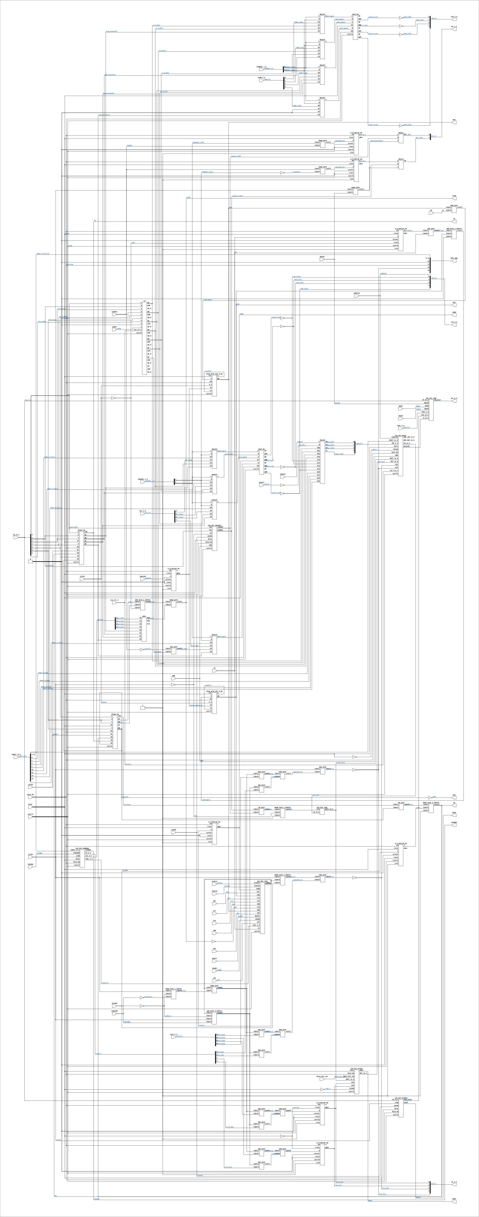
Contains: AND_GATE x10, AND_GATE_4_INPUTS, CGA_MIC_CONDREG, CGA_MIC_CSEL, CGA_MIC_IINC, CGA_MIC_INCOUNT, CGA_MIC_IPOS, CGA_MIC_MASEL, CGA_MIC_STACK, CGA_MIC_WCAREG, CMP4, D_FLIPFLOP_EN x8, L8, M169C_EN x2, MUX21L x2, MUX34P, MUX41P x8, NAND_GATE x5, NAND_GATE_3_INPUTS x4, NOR_GATE x7, NOR_GATE_3_INPUTS x2, OR_GATE x2, R41P_EN x2, SCAN_WITH_SET_N_EN x2
Module hierarchy - All modules
Schematic
Drawn from the Verilog: the yosys netlist of the Simulation (Verilator) build, instance CORE.CPU_BOARD.CPU.PROC.CGA.DELILAH.MIC. Sub-modules are boxes (click the picture to open it full size; there every sub-module box links to its page, and every wire shows its Verilog name).
Description
ND120 CGA (CPU Gate Array / DELILAH) /CGA/MIC MIC Page 9-13 SHEET 1 of 4 Last reviewed: 9-FEB-2025 Ronny Hansen
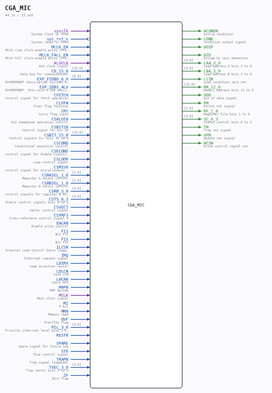
Ports
| Direction | Width | Name | Description |
|---|---|---|---|
| input | 1 |
sysclk |
System clock in FPGA |
| input | 1 |
sys_rst_n (active low) |
System reset in FPGA |
| input | 1 |
MCLK_EN |
MCLK rise clock-enable pulse (FPGA_FF_MODE, else 0) |
| input | 1 |
MCLK_FALL_EN |
MCLK fall clock-enable pulse (FPGA_FF_MODE, else 0) |
| input | 1 |
ALUCLK |
ALU clock signal |
| input | [15:0] |
CD_15_0 |
Data bus for communication |
| input | [6:0] |
EXP_FIDBO_6_0 |
EXPERIMENT (docs/serial-binload-300.md): internal |
| input | 1 |
EXP_IDBS_ALU |
EXPERIMENT: this word's IDB source is the ALU |
| input | 1 |
CFETCH |
Control signal for fetch operation |
| input | 1 |
CLFFN |
Clear flag function |
| input | 1 |
CRY |
Carry flag input |
| input | 1 |
CSALUI8 |
ALU immediate operation control |
| input | 1 |
CSBIT20 |
Control signal for bit 20 |
| input | [15:0] |
CSBIT_15_0 |
Control signals for bits 15 to 0 |
| input | 1 |
CSCOND |
Conditional execution control |
| input | 1 |
CSECOND |
Control signal for Enable Condition |
| input | 1 |
CSLOOP |
Loop control signal |
| input | 1 |
CSMIS0 |
Control signal for miscellaneous operation bit 0 |
| input | [1:0] |
CSRASEL_1_0 |
Register A select control |
| input | [1:0] |
CSRBSEL_1_0 |
Register B select control |
| input | [3:0] |
CSRB_3_0 |
Control signals for register B bits 3 to 0 |
| input | [3:0] |
CSTS_6_3 |
Status control signals bits 6 to 3 |
| input | 1 |
CSVECT |
Vector control signal |
| input | 1 |
CSXRF3 |
Cross-reference control signal 3 |
| input | 1 |
EWCAN |
Enable write control |
| input | 1 |
F11 |
Bit F11 |
| input | 1 |
F15 |
Bit F15 |
| input | 1 |
ILCSN |
Internal Load Control Store (negated) |
| input | 1 |
IRQ |
Interrupt request signal |
| input | 1 |
LDIRV |
Load direction vector |
| input | 1 |
LDLCN |
Load LCN |
| input | 1 |
LWCAN |
Latch WCA |
| input | 1 |
MAPN |
MAP Opcode |
| input | 1 |
MCLK |
Main clock signal |
| input | 1 |
MI |
M bit |
| input | 1 |
MRN |
Memory read |
| input | 1 |
OVF |
Overflow flag |
| input | [3:0] |
PIL_3_0 |
Priority interrupt level bits 3 to 0 |
| input | 1 |
RESTR |
|
| input | 1 |
SPARE |
Spare signal for future use |
| input | 1 |
STP |
Stop control signal |
| input | 1 |
TRAPN |
Trap signal (negated) |
| input | [3:0] |
TVEC_3_0 |
Trap vector bits 3 to 0 |
| input | 1 |
ZF |
Zero flag |
| output | 1 |
ACONDN |
Active condition |
| output | 1 |
COND |
Condition output signal |
| output | 1 |
DEEP |
|
| output | 1 |
DZD |
Divide by zero detection |
| output | [3:0] |
LAA_3_0 |
Load address A bits 3 to 0 |
| output | [3:0] |
LBA_3_0 |
Load address B bits 3 to 0 |
| output | 1 |
LCZN |
Load condition zero not |
| output | [12:0] |
MA_12_0 |
Memory address bits 12 to 0 |
| output | 1 |
OOD |
Out of data signal |
| output | 1 |
PN |
Parity not signal |
| output | [1:0] |
RF_1_0 |
Register file bits 1 to 0 |
| output | [3:0] |
SC_6_3 |
Status control bits 6 to 3 |
| output | 1 |
TN |
Trap not signal |
| output | 1 |
UPN |
Update not signal |
| output | 1 |
WCSN |
Write control signal not |
Verilog source
Verilog/DELILAH-CPU/CGA_MIC/circuit/CGA_MIC.v on GitHub.
Show the Verilog of CGA_MIC (1296 lines)
/**************************************************************************
** ND120 CGA (CPU Gate Array / DELILAH) **
** /CGA/MIC **
** MIC **
** **
** Page 9-13 **
** SHEET 1 of 4 **
** **
** Last reviewed: 9-FEB-2025 **
** Ronny Hansen **
***************************************************************************/
module CGA_MIC (
input sysclk, // System clock in FPGA
input sys_rst_n, // System reset in FPGA
input MCLK_EN, //! MCLK rise clock-enable pulse (FPGA_FF_MODE, else 0)
input MCLK_FALL_EN, //! MCLK fall clock-enable pulse (FPGA_FF_MODE, else 0)
input ALUCLK, //! ALU clock signal
input [15:0] CD_15_0, //! Data bus for communication
`ifdef ND120_EXP_LDIRV_PUSH
input [ 6:0] EXP_FIDBO_6_0, //! EXPERIMENT (docs/serial-binload-300.md): internal
//! IDB low bits, latched into IR on IDBS,ALU words
input EXP_IDBS_ALU, //! EXPERIMENT: this word's IDB source is the ALU
`endif
input CFETCH, //! Control signal for fetch operation
input CLFFN, //! Clear flag function
input CRY, //! Carry flag input
input CSALUI8, //! ALU immediate operation control
input CSBIT20, //! Control signal for bit 20
input [15:0] CSBIT_15_0, //! Control signals for bits 15 to 0
input CSCOND, //! Conditional execution control
input CSECOND, //! Control signal for Enable Condition
input CSLOOP, //! Loop control signal
input CSMIS0, //! Control signal for miscellaneous operation bit 0
input [ 1:0] CSRASEL_1_0, //! Register A select control
input [ 1:0] CSRBSEL_1_0, //! Register B select control
input [ 3:0] CSRB_3_0, //! Control signals for register B bits 3 to 0
input [ 3:0] CSTS_6_3, //! Status control signals bits 6 to 3
input CSVECT, //! Vector control signal
input CSXRF3, //! Cross-reference control signal 3
input EWCAN, //! Enable write control
input F11, //! Bit F11
input F15, //! Bit F15
input ILCSN, //! Internal Load Control Store (negated)
input IRQ, //! Interrupt request signal
input LDIRV, //! Load direction vector
input LDLCN, //! Load LCN
input LWCAN, //! Latch WCA
input MAPN, //! MAP Opcode
input MCLK, //! Main clock signal
input MI, //! M bit
input MRN, //! Memory read
input OVF, //! Overflow flag
input [ 3:0] PIL_3_0, //! Priority interrupt level bits 3 to 0
input RESTR, //!
input SPARE, //! Spare signal for future use
input STP, //! Stop control signal
input TRAPN, //! Trap signal (negated)
input [ 3:0] TVEC_3_0, //! Trap vector bits 3 to 0
input ZF, //! Zero flag
output ACONDN, //! Active condition
output COND, //! Condition output signal
output DEEP, //!
output DZD, //! Divide by zero detection
output [ 3:0] LAA_3_0, //! Load address A bits 3 to 0
output [ 3:0] LBA_3_0, //! Load address B bits 3 to 0
output LCZN, //! Load condition zero not
output [12:0] MA_12_0, //! Memory address bits 12 to 0
output OOD, //! Out of data signal
output PN, //! Parity not signal
output [ 1:0] RF_1_0, //! Register file bits 1 to 0
output [ 3:0] SC_6_3, //! Status control bits 6 to 3
output TN, //! Trap not signal
output UPN, //! Update not signal
output WCSN, //! Write control signal not
// DEBUG (Tang 06000-hang root-cause probe): the sequencer address-advance
// state, active-HIGH. bit15=SC6 bit14=s_mclk_n(regW mux-select, ~mclk_pa
// routed LEVEL) bit13=MCLK_EN(microsequencer clock-tick pulse)
// bit12:0=regIW (captured next-address). Shows which signal is FROZEN at the
// hang: MCLK_EN stuck-low => word never retires (mem/CYC); s_mclk_n stuck =>
// regW mux frozen; regIW stuck at 06000 vs jump target 0145.
output [15:0] XMIC_DBG
);
/*******************************************************************************
** The wires are defined here **
*******************************************************************************/
wire [ 1:0] s_csrasel_1_0;
wire [ 1:0] s_csrbsel_1_0;
wire [ 1:0] s_cswan_1_0;
wire [ 1:0] s_rf_1_0_out;
wire [ 3:0] s_csbit_15_12;
wire [ 3:0] s_csbit_3_0;
wire [ 3:0] s_csrb_3_0;
wire [ 3:0] s_csts_6_3;
wire [ 3:0] s_fs_6_3;
wire [ 3:0] s_jmp_3_0;
wire [ 3:0] s_laa_3_0_out;
wire [ 3:0] s_lba_3_0_out;
(* mark_debug = "true", DONT_TOUCH = "true" *) wire [ 3:0] s_lc_3_0;
wire [ 3:0] s_lcc_3_0;
wire [ 3:0] s_pil_3_0;
(* mark_debug = "true", DONT_TOUCH = "true" *) wire [ 3:0] s_sc_6_3_out;
wire [ 3:0] s_tsel_3_0;
wire [ 3:0] s_tvec_3_0;
wire [ 6:0] s_ir_6_0;
(* mark_debug = "true", DONT_TOUCH = "true" *) wire [12:0] s_iw_12_0;
(* mark_debug = "true", DONT_TOUCH = "true" *) wire [12:0] s_ma_12_0_out;
(* mark_debug = "true", DONT_TOUCH = "true" *) wire [12:0] s_next_12_0;
wire [12:0] s_ret_12_0;
(* mark_debug = "true", DONT_TOUCH = "true" *) wire [12:0] s_w_12_0;
(* mark_debug = "true", DONT_TOUCH = "true" *) wire [12:0] s_dbg_rep_12_0;
(* mark_debug = "true", DONT_TOUCH = "true" *) wire [12:0] s_dbg_jmp_12_0;
(* mark_debug = "true", DONT_TOUCH = "true" *) wire [12:0] s_wca_12_0;
wire [15:0] s_cd_15_0;
wire [15:0] s_csbit_15_0;
wire s_acond_n_out;
wire s_aluclk;
wire s_carry_in;
wire s_cfetch;
wire s_clff_n;
wire s_clff;
(* mark_debug = "true", DONT_TOUCH = "true" *) wire s_cond_n;
wire s_cond;
wire s_cry;
wire s_csalui8;
wire s_csbit20;
wire s_cscond;
wire s_csecond_n;
wire s_csecond;
wire s_csloop_n;
wire s_csloop;
wire s_csmis0;
wire s_csrasel1_n;
wire s_csvect_n;
wire s_csvect;
wire s_csxrf3_n;
wire s_csxrf3;
wire s_deep_out;
wire s_dzd_out;
wire s_dzd_signal;
wire s_dzdff_q;
(* mark_debug = "true", DONT_TOUCH = "true" *) wire s_ewca_n;
wire s_f11;
wire s_f15;
wire s_fs6_efalse;
wire s_csts5_etrue;
wire s_fs5_efalse;
wire s_csts4_etrue;
wire s_fs4_efalse;
wire s_csts3_etrue;
wire s_fs3_efalse;
wire s_gates18_out;
wire s_gates19_out;
wire s_gates20_out;
wire s_csfs_4;
wire s_csfs_3;
wire s_gates25_out;
wire s_gates28_out;
wire s_gates29_out;
wire s_gates3_out;
wire s_gates4_out;
wire s_gates5_out;
(* mark_debug = "true", DONT_TOUCH = "true" *) wire s_efalse;
(* mark_debug = "true", DONT_TOUCH = "true" *) wire s_etrue;
wire s_csts6_etrue;
wire s_gnd;
wire s_ialui8_clocked_qn;
wire s_icd_4;
wire s_icd_5;
wire s_irq;
wire s_iwan0or1;
wire s_laa_0_n_out;
wire s_laa_1_n_out;
wire s_laa_2_n_out;
wire s_laa_3_n_out;
wire s_laa0_signal;
wire s_laa1_signal;
wire s_laa2_signal;
wire s_laa3_d2_input;
wire s_laa3_signal;
wire s_lba_0_n_out;
wire s_lba_1_n_out;
wire s_lba_2_n_out;
wire s_lba_3_n_out;
wire s_lba0_signal;
wire s_lba1_signal;
wire s_lba2_signal;
wire s_lba3_signal;
wire s_lc_hi_con;
wire s_lcc_eq_lc;
wire s_lcs_n;
wire s_lcs;
wire s_lcsn_nand_ewcan;
wire s_lcz_n_out;
wire s_lcz;
wire s_ldirv;
wire s_ldlc_n;
wire s_loop;
wire s_lwca_n;
(* mark_debug = "true", DONT_TOUCH = "true" *) wire s_map_n;
wire s_mclk_n;
wire s_sclk_n;
wire s_clk_sc34; // Clock signal for flip-flop carrying SC3 and SC4 signal
wire s_mclk;
wire s_mi;
wire s_mrn;
wire s_ood_out;
wire s_ood_signal;
wire s_oodff_q;
wire s_ovf;
wire s_p_n_out;
wire s_power;
wire s_restr;
wire s_rf0_in_a;
wire s_rf1_in_a;
wire s_sc_3_out;
wire s_sc_4_out;
wire s_sc_5_n_out;
wire s_sc_6_n_out;
wire s_spare;
wire s_stp;
wire s_t_n_out;
(* mark_debug = "true", DONT_TOUCH = "true" *) wire s_trap_n;
wire s_up_n_out;
wire s_up_out;
wire s_wcs_n_out;
wire s_zf;
wire s_zfff_q_out;
/*******************************************************************************
** The module functionality is described here **
*******************************************************************************/
/*******************************************************************************
** Here all wiring is defined **
*******************************************************************************/
assign s_csbit_3_0[3:0] = s_csbit_15_0[3:0];
assign s_csbit_15_12[3:0] = s_csbit_15_0[15:12];
/*******************************************************************************
** Here all input connections are defined **
*******************************************************************************/
assign s_aluclk = ALUCLK;
assign s_cd_15_0[15:0] = CD_15_0;
assign s_cfetch = CFETCH;
assign s_clff_n = CLFFN;
assign s_cry = CRY;
assign s_csalui8 = CSALUI8;
assign s_csbit_15_0[15:0] = CSBIT_15_0;
assign s_csbit20 = CSBIT20;
assign s_cscond = CSCOND;
assign s_csecond = CSECOND;
assign s_csloop = CSLOOP;
assign s_csmis0 = CSMIS0;
assign s_csrasel_1_0[1:0] = CSRASEL_1_0;
assign s_csrb_3_0[3:0] = CSRB_3_0;
assign s_csrbsel_1_0[1:0] = CSRBSEL_1_0;
assign s_csts_6_3[3:0] = CSTS_6_3;
assign s_csvect = CSVECT;
assign s_csxrf3 = CSXRF3;
assign s_ewca_n = EWCAN;
assign s_f11 = F11;
assign s_f15 = F15;
assign s_irq = IRQ;
// In the schematic it goes through 2 inverting buffers, here we go direct. Not sure if its to get a small delay?
assign s_lcs_n = ILCSN;
assign s_ldirv = LDIRV;
assign s_ldlc_n = LDLCN;
assign s_lwca_n = LWCAN;
assign s_map_n = MAPN;
assign s_mclk = MCLK;
assign s_mi = MI;
assign s_mrn = MRN;
assign s_ovf = OVF;
assign s_pil_3_0[3:0] = PIL_3_0;
assign s_restr = RESTR;
assign s_spare = SPARE;
assign s_stp = STP;
assign s_trap_n = TRAPN;
assign s_tvec_3_0[3:0] = TVEC_3_0;
assign s_zf = ZF;
// P2 (docs/plan-fix-unconstrained-clocks.md): in FF mode the MCLK-
// clocked registers capture on posedge sysclk gated by MCLK_EN
// (aligned to the MCLK rise) instead of clocking on the routed net.
// Registers on the inverted nets (~MCLK) use MCLK_FALL_EN.
`ifdef FPGA_FF_MODE
localparam MCLK_CE = 1;
`else
localparam MCLK_CE = 0;
`endif
/*******************************************************************************
** Here all output connections are defined **
*******************************************************************************/
assign ACONDN = s_acond_n_out;
assign COND = s_cond;
assign DEEP = s_deep_out;
assign DZD = s_dzd_out;
assign LAA_3_0 = s_laa_3_0_out[3:0];
assign LBA_3_0 = s_lba_3_0_out[3:0];
assign LCZN = s_lcz_n_out;
assign MA_12_0 = s_ma_12_0_out[12:0];
assign OOD = s_ood_out;
assign PN = s_p_n_out;
assign RF_1_0 = s_rf_1_0_out[1:0];
assign SC_6_3 = s_sc_6_3_out[3:0];
assign TN = s_t_n_out;
assign UPN = s_up_n_out;
assign WCSN = s_wcs_n_out;
// DEBUG probe word: {SC6, s_mclk_n, MCLK_EN, regREP_comb[12:0]}. The Tang
// capture showed SC=JUMP + MCLK_EN pulsing but regIW frozen at 06000 (jump
// target 0145 never loaded). regREP_comb is the COMPUTED next-address (= the
// JUMP target when SC=JUMP). If regREP_comb=0145 here, the sequencer computes
// the jump correctly but regIW/regW never propagate it (capture/clocking bug);
// if regREP_comb=6000, the mux/jmpaddr is wrong. s_mclk_n = the routed ~mclk
// level that gates regW.
// bit15=CSBIT20 bit14=SC6 bit13=MCLK_EN bit12=0 bit11:0=CSBIT_11_0
// Tang measured s_jmpaddr=16000 = {csbit20=1, csbit_11_0[11:4]=0xC0}; 0xC00 =
// the ADDRESS 06000. So capture the RAW microword field CSBIT_11_0 that MASEL
// sees. Correct STZ word => CSBIT_11_0=0x065 (=> jmpaddr 0145). If instead
// CSBIT_11_0=0xC00 (=address 06000 low bits) => the WCS control-store READ is
// returning the ADDRESS not the DATA on silicon = ROOT CAUSE (WCS read path).
`ifdef ND_WD_TRACE_CSATRAP
assign XMIC_DBG = {s_tvec_3_0[3:0], s_trap_n, 11'b0};
`elsif ND_WD_TRACE_TVEC
// Same export as TANG_TRAP_CAPTURE below, under a second name so the trap
// dispatch can be ringed by the WINCHESTER dump path. TANG_TRAP_CAPTURE
// sits EARLIER in the capture-mode chain in ND120_TANG20K_TOP.v and would
// take the ring over completely, including its own CSA-stuck trigger, which
// never fires on a machine that is livelocking rather than stalled.
assign XMIC_DBG = {s_tvec_3_0[3:0], s_trap_n, 11'b0};
`elsif ND_WD_TRACE_TVEC_CSA
// ND_WD_TRACE_TVEC_CSA was missing from this chain, so a build using it got
// the sim-probe XMIC meanings from the `else` below and its ring recorded no
// trap vector at all. The top level reads s_xmic_dbg[15:11] = {TVEC, TRAPN}
// for BOTH its capture word and its falling-edge-of-TRAPN strobe
// (ND120_TANG20K_TOP.v:470 and :611), so it needs exactly the same export as
// the two modes above.
assign XMIC_DBG = {s_tvec_3_0[3:0], s_trap_n, 11'b0};
`elsif TANG_TRAP_CAPTURE
// Issue-D on-chip probe (Tang builds only; the sim never defines this, so the
// sim-probe XMIC bit meanings below are untouched): export the trap dispatch
// inputs this module already receives - {TVEC[3:0], TRAPN, 11'b0}. The Tang
// top combines bits 15:11 with CSA into the analyzer word (tang20k_defines.v).
assign XMIC_DBG = {s_tvec_3_0[3:0], s_trap_n, 11'b0};
`else
assign XMIC_DBG = {s_csbit20, s_sc_6_3_out[3], MCLK_EN, 1'b0, s_csbit_15_0[11:0]};
`endif
/*******************************************************************************
** Here all in-lined components are defined **
*******************************************************************************/
// Power
assign s_power = 1'b1;
// Ground
assign s_gnd = 1'b0;
// NOT Gate
assign s_clff = ~s_clff_n;
assign s_csecond_n = ~s_csecond;
assign s_csloop_n = ~s_csloop;
assign s_csrasel1_n = ~s_csrasel_1_0[1];
assign s_csvect_n = ~s_csvect;
assign s_csxrf3_n = ~s_csxrf3;
assign s_lcs = ~s_lcs_n;
assign s_laa_3_0_out[0] = ~s_laa_0_n_out;
assign s_laa_3_0_out[1] = ~s_laa_1_n_out;
assign s_laa_3_0_out[2] = ~s_laa_2_n_out;
assign s_laa_3_0_out[3] = ~s_laa_3_n_out;
assign s_lba_3_0_out[0] = ~s_lba_0_n_out;
assign s_lba_3_0_out[1] = ~s_lba_1_n_out;
assign s_lba_3_0_out[2] = ~s_lba_2_n_out;
assign s_lba_3_0_out[3] = ~s_lba_3_n_out;
assign s_lcz = ~s_lcz_n_out;
assign s_mclk_n = ~s_mclk; // MASEL clock (negated MCLK)
assign s_sclk_n = ~s_mclk; // STACK CLOCK (nedgated MCLK)
assign s_clk_sc34 = ~s_mclk; // Will be nagated at the chip level
assign s_sc_6_3_out[0] = s_sc_3_out;
assign s_sc_6_3_out[1] = s_sc_4_out;
assign s_sc_6_3_out[2] = ~s_sc_5_n_out;
assign s_sc_6_3_out[3] = ~s_sc_6_n_out;
assign s_up_n_out = ~s_up_out;
/*******************************************************************************
** Here all normal components are defined **
*******************************************************************************/
OR_GATE #(
.BubblesMask(2'b00)
) GATES_1 (
.input1(s_cswan_1_0[1]),
.input2(s_cswan_1_0[0]),
.result(s_iwan0or1)
);
NAND_GATE_3_INPUTS #(
.BubblesMask(3'b000)
) GATES_2 (
.input1(s_iwan0or1),
.input2(s_lcs),
.input3(s_power),
.result(s_carry_in)
);
NOR_GATE_3_INPUTS #(
.BubblesMask(3'b000)
) GATES_3 (
.input1(s_icd_4),
.input2(s_icd_5),
.input3(s_clff),
.result(s_gates3_out)
);
OR_GATE #(
.BubblesMask(2'b00)
) GATES_4 (
.input1(s_lc_hi_con),
.input2(s_up_out),
.result(s_gates4_out)
);
NAND_GATE_3_INPUTS #(
.BubblesMask(3'b000)
) GATES_5 (
.input1(s_lcs_n),
.input2(s_csloop_n),
.input3(s_csecond_n),
.result(s_gates5_out)
);
AND_GATE_4_INPUTS #(
.BubblesMask(4'h0)
) GATES_6 (
.input1(s_cond_n),
.input2(s_csloop_n),
.input3(s_lcs_n),
.input4(s_csecond),
.result(s_efalse)
);
NAND_GATE_3_INPUTS #(
.BubblesMask(3'b000)
) GATES_7 (
.input1(s_gates4_out),
.input2(s_loop),
.input3(s_power),
.result(s_p_n_out)
);
NAND_GATE #(
.BubblesMask(2'b00)
) GATES_8 (
.input1(s_cond_n),
.input2(s_gates5_out),
.result(s_etrue)
);
AND_GATE #(
.BubblesMask(2'b00)
) GATES_9 (
.input1(s_etrue),
.input2(s_csts_6_3[3]),
.result(s_csts6_etrue)
);
AND_GATE #(
.BubblesMask(2'b00)
) GATES_10 (
.input1(s_efalse),
.input2(s_fs_6_3[3]),
.result(s_fs6_efalse)
);
AND_GATE #(
.BubblesMask(2'b00)
) GATES_11 (
.input1(s_etrue),
.input2(s_csts_6_3[2]),
.result(s_csts5_etrue)
);
AND_GATE #(
.BubblesMask(2'b00)
) GATES_12 (
.input1(s_efalse),
.input2(s_fs_6_3[2]),
.result(s_fs5_efalse)
);
AND_GATE #(
.BubblesMask(2'b00)
) GATES_13 (
.input1(s_etrue),
.input2(s_csts_6_3[1]),
.result(s_csts4_etrue)
);
AND_GATE #(
.BubblesMask(2'b00)
) GATES_14 (
.input1(s_efalse),
.input2(s_fs_6_3[1]),
.result(s_fs4_efalse)
);
AND_GATE #(
.BubblesMask(2'b00)
) GATES_15 (
.input1(s_etrue),
.input2(s_csts_6_3[0]),
.result(s_csts3_etrue)
);
AND_GATE #(
.BubblesMask(2'b00)
) GATES_16 (
.input1(s_efalse),
.input2(s_fs_6_3[0]),
.result(s_fs3_efalse)
);
NAND_GATE #(
.BubblesMask(2'b00)
) GATES_17 (
.input1(s_gates3_out),
.input2(s_lcc_eq_lc),
.result(s_lcz_n_out)
);
NAND_GATE_3_INPUTS #(
.BubblesMask(3'b000)
) GATES_18 (
.input1(s_lcs_n),
.input2(s_cond_n),
.input3(s_csloop),
.result(s_gates18_out)
);
NOR_GATE #(
.BubblesMask(2'b00)
) GATES_19 (
.input1(s_csts6_etrue),
.input2(s_fs6_efalse),
.result(s_gates19_out)
);
NOR_GATE #(
.BubblesMask(2'b00)
) GATES_20 (
.input1(s_csts5_etrue),
.input2(s_fs5_efalse),
.result(s_gates20_out)
);
NOR_GATE #(
.BubblesMask(2'b00)
) GATES_21 (
.input1(s_csts4_etrue),
.input2(s_fs4_efalse),
.result(s_csfs_4)
);
NOR_GATE #(
.BubblesMask(2'b00)
) GATES_22 (
.input1(s_csts3_etrue),
.input2(s_fs3_efalse),
.result(s_csfs_3)
);
NOR_GATE #(
.BubblesMask(2'b11)
) GATES_23 (
.input1(s_lcs_n),
.input2(s_gates19_out),
.result(s_sc_6_n_out)
);
NOR_GATE #(
.BubblesMask(2'b11)
) GATES_24 (
.input1(s_gates18_out),
.input2(s_gates20_out),
.result(s_sc_5_n_out)
);
AND_GATE #(
.BubblesMask(2'b00)
) GATES_25 (
.input1(s_zfff_q_out),
.input2(s_zf),
.result(s_gates25_out)
);
NOR_GATE_3_INPUTS #(
.BubblesMask(3'b000)
) GATES_26 (
.input1(s_gates25_out),
.input2(s_dzd_out),
.input3(s_gnd),
.result(s_dzd_signal)
);
NOR_GATE #(
.BubblesMask(2'b00)
) GATES_27 (
.input1(s_ood_out),
.input2(s_mi),
.result(s_ood_signal)
);
NAND_GATE #(
.BubblesMask(2'b00)
) GATES_28 (
.input1(s_csrasel_1_0[0]),
.input2(s_csxrf3),
.result(s_gates28_out)
);
NAND_GATE #(
.BubblesMask(2'b00)
) GATES_29 (
.input1(s_csxrf3),
.input2(s_csrasel1_n),
.result(s_gates29_out)
);
AND_GATE #(
.BubblesMask(2'b00)
) GATES_30 (
.input1(s_csxrf3_n),
.input2(s_ir_6_0[6]),
.result(s_laa3_d2_input)
);
NAND_GATE #(
.BubblesMask(2'b00)
) GATES_31 (
.input1(s_lcs_n),
.input2(s_ewca_n),
.result(s_lcsn_nand_ewcan)
);
// MCLK domain: clocked on posedge s_mclk
D_FLIPFLOP_EN #(
.USE_ENABLE(MCLK_CE)
) MEMORY_33 (
.sysclk(sysclk),
.EN(MCLK_EN),
.clock(s_mclk),
.d(s_csloop),
.preset(1'b0),
.q(s_loop),
.qBar(),
.reset(1'b0),
.tick(1'b1)
);
// MCLK domain: InvertClockEnable(1) on s_clk_sc34 (= ~MCLK) fires on the
// falling edge of ~MCLK, i.e. the MCLK rising edge -> MCLK_EN.
// (D_FLIPFLOP_EN has no InvertClockEnable, so the latch-mode original
// is kept verbatim in the else branch.)
`ifdef FPGA_FF_MODE
D_FLIPFLOP_EN #(
.USE_ENABLE(MCLK_CE)
) MEMORY_34 (
.sysclk(sysclk),
.EN(MCLK_EN),
.clock(s_clk_sc34),
.d(s_csfs_3),
.preset(1'b0),
.q(),
.qBar(s_sc_3_out),
.reset(1'b0),
.tick(1'b1)
);
`else
D_FLIPFLOP #(
.InvertClockEnable(1)
) MEMORY_34 (
.clock(s_clk_sc34),
.d(s_csfs_3),
.preset(1'b0),
.q(),
.qBar(s_sc_3_out),
.reset(1'b0),
.tick(1'b1)
);
`endif
// MCLK domain: clocked on posedge s_mclk (async clear s_clff)
D_FLIPFLOP_EN #(.USE_ENABLE(MCLK_CE), .ASYNC_RESET(1)
) MEMORY_35 (
.sysclk(sysclk),
.EN(MCLK_EN),
.clock(s_mclk),
.d(s_zf),
.preset(1'b0),
.q(s_zfff_q_out),
.qBar(),
.reset(s_clff),
.tick(1'b1)
);
// MCLK domain: clocked on posedge s_mclk
D_FLIPFLOP_EN #(
.USE_ENABLE(MCLK_CE)
) MEMORY_36 (
.sysclk(sysclk),
.EN(MCLK_EN),
.clock(s_mclk),
.d(s_csalui8),
.preset(1'b0),
.q(),
.qBar(s_ialui8_clocked_qn),
.reset(1'b0),
.tick(1'b1)
);
// MCLK domain: InvertClockEnable(1) on s_clk_sc34 (= ~MCLK) fires on the
// falling edge of ~MCLK, i.e. the MCLK rising edge -> MCLK_EN.
// (D_FLIPFLOP_EN has no InvertClockEnable, so the latch-mode original
// is kept verbatim in the else branch.)
`ifdef FPGA_FF_MODE
D_FLIPFLOP_EN #(
.USE_ENABLE(MCLK_CE)
) MEMORY_37 (
.sysclk(sysclk),
.EN(MCLK_EN),
.clock(s_clk_sc34),
.d(s_csfs_4),
.preset(1'b0),
.q(),
.qBar(s_sc_4_out),
.reset(1'b0),
.tick(1'b1)
);
`else
D_FLIPFLOP #(
.InvertClockEnable(1)
) MEMORY_37 (
.clock(s_clk_sc34),
.d(s_csfs_4),
.preset(1'b0),
.q(),
.qBar(s_sc_4_out),
.reset(1'b0),
.tick(1'b1)
);
`endif
// MCLK domain: clocked on posedge s_mclk
D_FLIPFLOP_EN #(
.USE_ENABLE(MCLK_CE)
) MEMORY_38 (
.sysclk(sysclk),
.EN(MCLK_EN),
.clock(s_mclk),
.d(s_gates29_out),
.preset(1'b0),
.q(s_rf1_in_a),
.qBar(),
.reset(1'b0),
.tick(1'b1)
);
// MCLK domain: clocked on posedge s_mclk
D_FLIPFLOP_EN #(
.USE_ENABLE(MCLK_CE)
) MEMORY_39 (
.sysclk(sysclk),
.EN(MCLK_EN),
.clock(s_mclk),
.d(s_gates28_out),
.preset(1'b0),
.q(s_rf0_in_a),
.qBar(),
.reset(1'b0),
.tick(1'b1)
);
/*******************************************************************************
** Here all sub-circuits are defined **
*******************************************************************************/
CGA_MIC_INCOUNT MIC_INCOUNT (
.sysclk(sysclk),
.MCLK_EN(MCLK_EN),
.CD0(s_cd_15_0[0]),
.CD1(s_cd_15_0[1]),
.CSWAN0(s_cswan_1_0[0]),
.CSWAN1(s_cswan_1_0[1]),
.EC(s_lcs),
.LWCAN(s_lwca_n),
.MCLK(s_mclk),
.MRN(s_mrn)
);
// Debug (to see the value of the loop counter when debugging micro-code)
(* keep = "true", DONT_TOUCH = "true" *) wire [5:0] loop_counter;
assign loop_counter[5:0] = {s_icd_5, s_icd_4,s_lc_3_0[3],s_lc_3_0[2],s_lc_3_0[1],s_lc_3_0[0]};
// MCLK domain: CP = s_mclk, counts on posedge MCLK
M169C_EN #(.USE_ENABLE(MCLK_CE)) LC_HI (
.sysclk(sysclk),
.EN(MCLK_EN),
.CP(s_mclk),
.A(s_cd_15_0[4]),
.B(s_cd_15_0[5]),
.C(s_cd_15_0[5]),
.D(s_cd_15_0[5]),
.CON(s_lc_hi_con),
.NL(s_ldlc_n),
.PN(s_p_n_out),
.QA(s_icd_4),
.QB(s_icd_5),
.QC(),
.QD(s_up_out),
.TN(s_t_n_out),
.UP(s_up_out)
);
// MCLK domain: CP = s_mclk, counts on posedge MCLK
M169C_EN #(.USE_ENABLE(MCLK_CE)) LC_LO (
.sysclk(sysclk),
.EN(MCLK_EN),
.CP(s_mclk),
.A(s_cd_15_0[0]),
.B(s_cd_15_0[1]),
.C(s_cd_15_0[2]),
.D(s_cd_15_0[3]),
.CON(s_t_n_out),
.NL(s_ldlc_n),
.PN(s_p_n_out),
.QA(s_lc_3_0[0]),
.QB(s_lc_3_0[1]),
.QC(s_lc_3_0[2]),
.QD(s_lc_3_0[3]),
.TN(s_gnd),
.UP(s_up_out)
);
MUX21L M_RF1 (
.A (s_rf1_in_a),
.B (s_cswan_1_0[1]),
.S (s_lcsn_nand_ewcan),
.ZN(s_rf_1_0_out[1])
);
MUX21L M_RF0 (
.A (s_rf0_in_a),
.B (s_cswan_1_0[0]),
.S (s_lcsn_nand_ewcan),
.ZN(s_rf_1_0_out[0])
);
MUX34P ILC_MUX
(
// Input signals
.A (s_csmis0),
.B (s_csvect_n),
.D00(s_ir_6_0[0]),
.D01(s_ir_6_0[1]),
.D02(s_ir_6_0[2]),
.D03(s_ir_6_0[3]),
.D10(s_laa_3_0_out[0]),
.D11(s_laa_3_0_out[1]),
.D12(s_laa_3_0_out[2]),
.D13(s_laa_3_0_out[3]),
.D20(s_csbit_3_0[0]),
.D21(s_csbit_3_0[1]),
.D22(s_csbit_3_0[2]),
.D23(s_csbit_3_0[3]),
// Output signals
.Z0 (s_jmp_3_0[0]),
.Z1 (s_jmp_3_0[1]),
.Z2 (s_jmp_3_0[2]),
.Z3 (s_jmp_3_0[3])
);
`ifdef ND120_EXP_LDIRV_PUSH
// EXPERIMENT rule 2 (docs/serial-binload-300.md): load IR from the
// internal IDB on every IDBS,ALU word (CSIDBS==0). The decisive load
// point is o500 in IOXG (IDB = masked device address), which vectors
// poll/read/activate/macro-IOX/IOXT/BAUDS alike; o501-o503 use
// BARG/ARG IDB sources and so preserve it. IOXT2's explicit
// COMM,LDIRV covers the IOXX1 entry that skips o500. Qualified to
// the MCLK-low phase like the real LDIRV decode.
wire s_exp_alu_ld = EXP_IDBS_ALU & s_mclk_n;
wire s_exp_irgate = s_ldirv | s_exp_alu_ld;
wire [6:0] s_exp_irdata = s_exp_alu_ld ? EXP_FIDBO_6_0 : s_cd_15_0[6:0];
L8 IRLATCH
(
// System Input signals
.sysclk(sysclk), // System clock in FPGA
.sys_rst_n(sys_rst_n), // System reset in FPGA
.L (s_exp_irgate),
// Input signals
.A (s_exp_irdata[0]),
.B (s_exp_irdata[1]),
.C (s_exp_irdata[2]),
.D (s_exp_irdata[3]),
.E (s_exp_irdata[4]),
.F (s_exp_irdata[5]),
.G (s_exp_irdata[6]),
.H (1'b0),
`else
L8 IRLATCH
(
// System Input signals
.sysclk(sysclk), // System clock in FPGA
.sys_rst_n(sys_rst_n), // System reset in FPGA
.L (s_ldirv),
// Input signals
.A (s_cd_15_0[0]),
.B (s_cd_15_0[1]),
.C (s_cd_15_0[2]),
.D (s_cd_15_0[3]),
.E (s_cd_15_0[4]),
.F (s_cd_15_0[5]),
.G (s_cd_15_0[6]),
.H (1'b0),
`endif
// Output signals
.QA (s_ir_6_0[0]),
.QAN(),
.QB (s_ir_6_0[1]),
.QBN(),
.QC (s_ir_6_0[2]),
.QCN(),
.QD (s_ir_6_0[3]),
.QDN(),
.QE (s_ir_6_0[4]),
.QEN(),
.QF (s_ir_6_0[5]),
.QFN(),
.QG (s_ir_6_0[6]),
.QGN(),
.QH (),
.QHN(),
// registered-value taps: deliberately unconnected here -
// the transparent output is the wanted one (see L8/L4 header).
.QA_R(),
.QB_R(),
.QC_R(),
.QD_R(),
.QE_R(),
.QF_R(),
.QG_R(),
.QH_R()
);
CGA_MIC_CONDREG CONDREG (
.sysclk(sysclk),
.MCLK_EN(MCLK_EN),
// Input
.CSBIT_11_0(s_csbit_15_0[11:0]),
.CSSCOND(s_cscond),
.LCSN(s_lcs_n),
.MCLK(s_mclk),
// Output
.LCC_3_0(s_lcc_3_0[3:0]),
.FS_6_3(s_fs_6_3[3:0]),
.TSEL_3_0(s_tsel_3_0[3:0]),
.ACONDN(s_acond_n_out)
);
// A Operand
/********* LAA 3:0 ************/
MUX41P M_LAA_3 (
.A (s_csrasel_1_0[0]),
.B (s_csrasel_1_0[1]),
.D0(s_csbit_15_12[3]),
.D1(s_pil_3_0[3]),
.D2(s_laa3_d2_input),
.D3(s_lc_3_0[3]),
.Z (s_laa3_signal)
);
MUX41P M_LAA_2 (
.A (s_csrasel_1_0[0]),
.B (s_csrasel_1_0[1]),
.D0(s_csbit_15_12[2]),
.D1(s_pil_3_0[2]),
.D2(s_ir_6_0[5]),
.D3(s_lc_3_0[2]),
.Z (s_laa2_signal)
);
MUX41P M_LAA_1 (
.A (s_csrasel_1_0[0]),
.B (s_csrasel_1_0[1]),
.D0(s_csbit_15_12[1]),
.D1(s_pil_3_0[1]),
.D2(s_ir_6_0[4]),
.D3(s_lc_3_0[1]),
.Z (s_laa1_signal)
);
MUX41P M_LAA_0 (
.A (s_csrasel_1_0[0]),
.B (s_csrasel_1_0[1]),
.D0(s_csbit_15_12[0]),
.D1(s_pil_3_0[0]),
.D2(s_ir_6_0[3]),
.D3(s_lc_3_0[0]),
.Z (s_laa0_signal)
);
// MCLK domain: CP = s_mclk, clocked on posedge MCLK
R41P_EN #(.USE_ENABLE(MCLK_CE)) LAA_REG (
.sysclk(sysclk),
.EN(MCLK_EN),
.CP(s_mclk),
.A(s_laa0_signal),
.B(s_laa1_signal),
.C(s_laa2_signal),
.D(s_laa3_signal),
.QA (),
.QAN(s_laa_0_n_out),
.QB (),
.QBN(s_laa_1_n_out),
.QC (),
.QCN(s_laa_2_n_out),
.QD (),
.QDN(s_laa_3_n_out)
);
// B Operand
/********** LBA 3:0 **************/
MUX41P M_LBA_3 (
.A (s_csrbsel_1_0[0]),
.B (s_csrbsel_1_0[1]),
.D0(s_csrb_3_0[3]),
.D1(s_gnd),
.D2(s_gnd),
.D3(s_lc_3_0[3]),
.Z (s_lba3_signal)
);
MUX41P M_LBA_2 (
.A (s_csrbsel_1_0[0]),
.B (s_csrbsel_1_0[1]),
.D0(s_csrb_3_0[2]),
.D1(s_ir_6_0[2]),
.D2(s_ir_6_0[5]),
.D3(s_lc_3_0[2]),
.Z (s_lba2_signal)
);
MUX41P M_LBA_1 (
.A (s_csrbsel_1_0[0]),
.B (s_csrbsel_1_0[1]),
.D0(s_csrb_3_0[1]),
.D1(s_ir_6_0[1]),
.D2(s_ir_6_0[4]),
.D3(s_lc_3_0[1]),
.Z (s_lba1_signal)
);
MUX41P M_LBA_0 (
.A (s_csrbsel_1_0[0]),
.B (s_csrbsel_1_0[1]),
.D0(s_csrb_3_0[0]),
.D1(s_ir_6_0[0]),
.D2(s_ir_6_0[3]),
.D3(s_lc_3_0[0]),
.Z (s_lba0_signal)
);
// MCLK domain: CP = s_mclk, clocked on posedge MCLK
R41P_EN #(.USE_ENABLE(MCLK_CE)) LBA_REG (
.sysclk(sysclk),
.EN(MCLK_EN),
.CP(s_mclk),
.A(s_lba0_signal),
.B(s_lba1_signal),
.C(s_lba2_signal),
.D(s_lba3_signal),
.QA (),
.QAN(s_lba_0_n_out),
.QB (),
.QBN(s_lba_1_n_out),
.QC (),
.QCN(s_lba_2_n_out),
.QD (),
.QDN(s_lba_3_n_out)
);
/*********/
CMP4 LC_CMP (
.A0 (s_lcc_3_0[0]),
.A1 (s_lcc_3_0[1]),
.A2 (s_lcc_3_0[2]),
.A3 (s_lcc_3_0[3]),
.AEB(s_lcc_eq_lc),
.AGB(),
.ALB(),
.B0 (s_lc_3_0[0]),
.B1 (s_lc_3_0[1]),
.B2 (s_lc_3_0[2]),
.B3 (s_lc_3_0[3])
);
CGA_MIC_IINC MIC_IINC (
.CIN(s_carry_in),
.IW_12_0(s_iw_12_0[12:0]),
.NEXT_12_0(s_next_12_0[12:0])
);
CGA_MIC_STACK MIC_STACK (
.sysclk(sysclk),
.MCLK_EN(MCLK_EN),
.MCLK_FALL_EN(MCLK_FALL_EN),
// Input
.MCLK (s_mclk),
.SCLKN(s_sclk_n), //Stack Clock (Negated MCLK)
.SC3 (s_sc_6_3_out[0]), // SC[4:3] values - 00:HOLD, 01:POP, 10:LOAD, 11:PUSH
.SC4 (s_sc_6_3_out[1]), //
.NEXT_12_0(s_next_12_0[12:0]),
// Output
.DEEP(s_deep_out),
.RET_12_0(s_ret_12_0[12:0])
);
CGA_MIC_MASEL MIC_MASEL (
.sysclk(sysclk), // System clock in FPGA
.sys_rst_n(sys_rst_n), // System reset in FPGA
.MCLK_EN(MCLK_EN),
// Input signals
.CSBIT20(s_csbit20),
.CSBIT_11_0(s_csbit_15_0[11:0]),
.JMP_3_0(s_jmp_3_0[3:0]),
.MCLK(s_mclk),
.MCLKN(s_mclk_n),
.MRN(s_mrn),
.NEXT_12_0(s_next_12_0[12:0]),
.RET_12_0(s_ret_12_0[12:0]),
.SC5(s_sc_6_3_out[2]),
.SC6(s_sc_6_3_out[3]),
// Output signals
.IW_12_0(s_iw_12_0[12:0]),
.W_12_0(s_w_12_0[12:0]),
.DBG_REP_12_0(s_dbg_rep_12_0[12:0]),
.DBG_JMP_12_0(s_dbg_jmp_12_0[12:0])
);
// MCLK domain: CLK = s_mclk, clocked on posedge MCLK (async set S_n)
SCAN_WITH_SET_N_EN #(.USE_ENABLE(MCLK_CE)) OOD_FF (
.sysclk(sysclk),
.EN(MCLK_EN),
.CLK(s_mclk),
.D (s_ood_signal),
.Q (s_oodff_q),
.QN (s_ood_out),
.S_n(s_clff_n),
.TE (s_ialui8_clocked_qn),
.TI (s_oodff_q)
);
// MCLK domain: CLK = s_mclk, clocked on posedge MCLK (async set S_n)
SCAN_WITH_SET_N_EN #(.USE_ENABLE(MCLK_CE)) DZD_FF (
.sysclk(sysclk),
.EN(MCLK_EN),
.CLK(s_mclk),
.D (s_dzd_signal),
.Q (s_dzdff_q),
.QN (s_dzd_out),
.S_n(s_clff_n),
.TE (s_ialui8_clocked_qn),
.TI (s_dzdff_q)
);
CGA_MIC_WCAREG MIC_WCAREG (
.sysclk(sysclk),
.MCLK_EN(MCLK_EN),
.CD_15_0(s_cd_15_0[15:0]),
.LCSN(s_lcs_n),
.LWCAN(s_lwca_n),
.MCLK(s_mclk),
.WCA_12_0(s_wca_12_0[12:0]),
.WCSN(s_wcs_n_out)
);
CGA_MIC_IPOS MIC_IPOS (
// Inputs
.CD_15_0(s_cd_15_0[15:0]),
.EWCAN(s_ewca_n),
.MAPN(s_map_n),
.TRAPN(s_trap_n),
.TVEC_3_0(s_tvec_3_0[3:0]),
.WCA_12_0(s_wca_12_0[12:0]),
.W_12_0(s_w_12_0[12:0]),
// Outputs
.MA_12_0(s_ma_12_0_out[12:0])
);
CGA_MIC_CSEL CSEL (
// Input
.sysclk(sysclk),
.ALUCLK(s_aluclk),
.CFETCH(s_cfetch),
.COND(s_cond),
.CRY(s_cry),
.DZD(s_dzd_out),
.F11(s_f11),
.F15(s_f15),
.IRQ(s_irq),
.LCZ(s_lcz),
.OOD(s_ood_out),
.OVF(s_ovf),
.RESTR(s_restr),
.SPARE(s_spare),
.STP(s_stp),
.TSEL_3_0(s_tsel_3_0[3:0]),
.ZF(s_zf),
// Output
.CONDN(s_cond_n)
);
// MCLK domain: clocked on posedge s_mclk
D_FLIPFLOP_EN #(
.USE_ENABLE(MCLK_CE)
) MEMORY_32 (
.sysclk(sysclk),
.EN(MCLK_EN),
.clock(s_mclk),
.d(s_cond_n),
.preset(1'b0),
.q(),
.qBar(s_cond),
.reset(1'b0),
.tick(1'b1)
);
endmodule